In this application note, Würth Elektronik deals in detail with blocking capacitors, which filter out higher frequencies from the signal path by deriving RF signals superimposing a DC current against ground.
The article written by Field Application Engineer Andreas Nadler brings a useful design tips how to reduce RF interference currents most effectively using real measurements and practically realistic simulations.
PCB-layout techniques for filter and blocking capacitors are also described that are ideally suited for the supply pins of digital ICs. Published on Passive Components Blog under permission.
INTRODUCTION
The fundamental task of blocking capacitors on supply pins is basically to short-circuit the clocked current loop of the digital circuits locally using a low impedance.
This reduces the radiated magnetic field strength and the RF interference currents coupled into the supply voltage level as much as possible. If the capacitors are optimally selected with regard to their impedance curve and geometrically optimally placed at the VCC pins, then the clocked RF current can be blocked in the best possible way.
In the general technical literature much can be found about correct PCB layout techniques, multi-stage filters and blocking capacitors for supply pins of digital ICs. However, real measurements or practical simulations are often missing. The goal of this Application Note is to show the influence of design, the number of ground vias and the placement of the MLCC filter components to each other. Furthermore, it will be shown that an unfortunate dimensioning of capacitor banks can cause more problems than initially expected.
Blocking capacitors at supply pins have the task to close the clocked current loop of the digital circuits locally in the shortest way with the help of a low impedance. This reduces the radiated magnetic field strength and the RF interference currents coupled into the supply voltage level as much as possible. If the capacitors are optimally selected with regard to their impedance curve and geometrically optimally placed at the VCC pins, then the clocked RF current can be blocked in the best possible way.
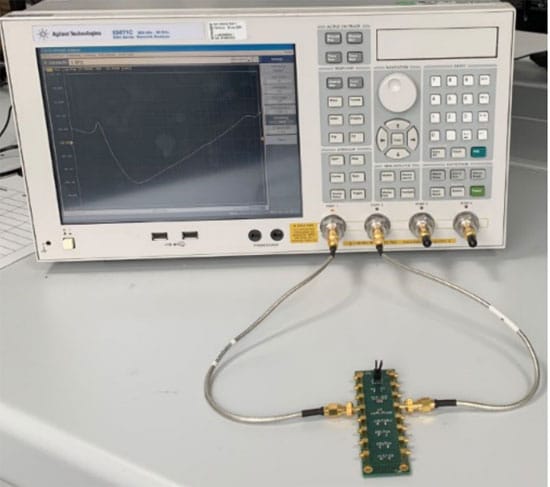
To demonstrate the various influences in practice, the insertion loss S21 was determined over a wide frequency range from 300 kHz to 3 GHz using a 4-layer PCB designed for exactly 50 Ω impedance. In addition, two supporting simulations were created using the freeware LTspice and the professional tool EMCoS. This was to determine how close one can get to the real measurement using E5071C (ENA RF Network Analyzer) and what influence the via positioning has relative to each other. The MMCX connector types of Würth Elektronik eiCan were selected as RF connectors.
CIRCUIT DIAGRAM AND MEASUREMENT SETUP
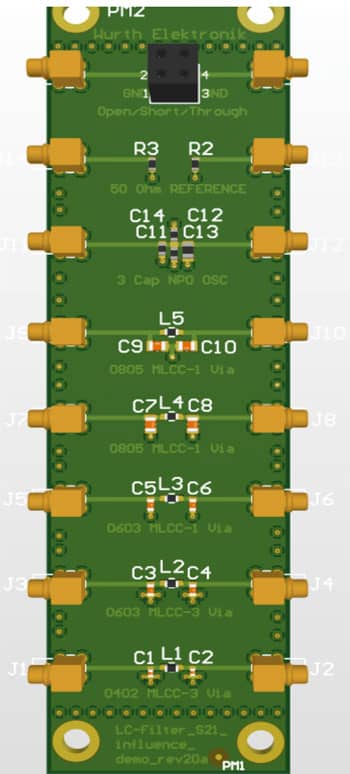
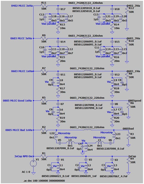
The demo board in Figure 1 has 6 measuring channels. The schematic of the demo board is shown in Figure 2.
The measurement setup with the network analyzer is shown in Figure 3. The top two are for calibration of the measurement setup. The third channel is for measuring the oscillation which occurs when several MLCCs are connected in parallel. In addition, it is to be compared to what extent class 1 NP0/C0G differs from class 2 X5R/X7R ceramics with otherwise identical component values. In the remaining 5 channels always the same 0603 HF SMD ferrite 742863122 and two 100 nF X7R MLCCs each are used. However, differences can be found in the number of GND vias, the design and in the geometrical arrangement of the MLCCs.
Basically, the higher and more broadband the insertion loss S21 is, the better the effect of the entire filter and/or the individual blocking capacitor.
Since the same ferrite and two 100 nF MLCCs are placed everywhere in all 6 measurement channels, the insertion loss in the measurements depends on:
- Design of the MLCCs (especially their ESL)
- Number of vias to GND (more vias = lower parasitic inductance to GND)
- Arrangement of MLCCs to ferrite (parasitic inductive & capacitive coupling)
- Length of the traces to the MLCC pads (adds up to the ESL of the MLCC)
LAYOUT IN DETAIL
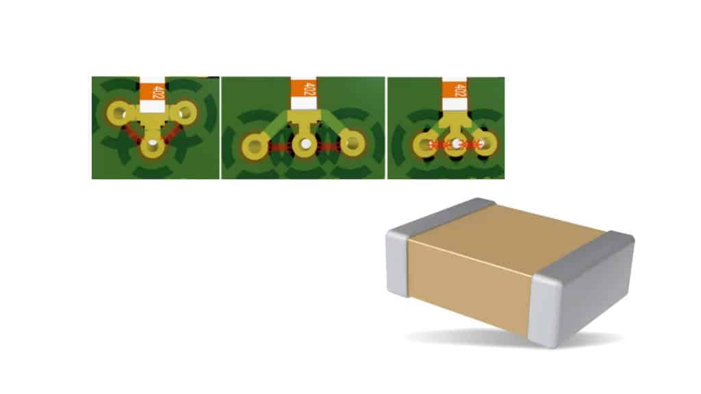
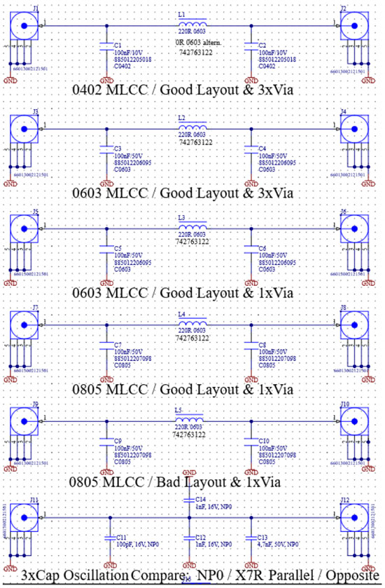
In advance, the smallest MLCC designs, 0403, with 3 vias per GND pad, are expected to give the best result because their equivalent series inductance (ESL) is the smallest (Figure 4).
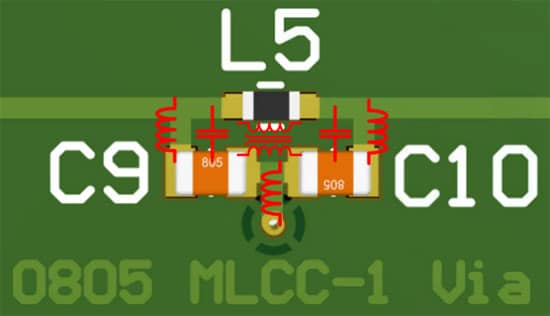
The largest MLCC designs, 0805 with only one via per GND pad are expected to have significantly worse insertion loss above the resonant frequency (Figure 5).


The worst result is expected from the measurement channel with the 0805 MLCCs in combination with the poor layout (Figure 6). Here, only a single GND via was used for both MLCCs GND pads. In addition, the MLCCs are arranged in parallel with the ferrite, resulting in parasitic inductive and capacitive couplings. Furthermore, the trace connections of the MLCC pads are unnecessarily long. 1-2 mm in length corresponds to approximately 0.5 nH of additional ESL. Figure 7 illustrates the parasitic impedances caused by the design and layout.

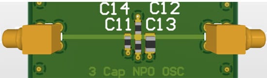
For the measurement channels with the capacitors of the 0603 types, results are expected which lie between the 0402 and 0805 types. In addition, a measurement channel was designed to investigate the effects of several MLCC capacitors of class 1 ceramic (NP0/C0G) with different capacitances connected in parallel. In this comparison, one 100 pF, one 1 nF and one 4.7 nF were selected. Since these are particularly high Q capacitors, where the dielectric is titanium oxide, unfavorable resonances between the various capacitive and inductive elements of the capacitors are expected. These resonances would greatly reduce the insertion loss S21 in certain frequency ranges. Furthermore, the same experiment was performed with MLCCs with class 2 ceramics (X7R). X7R ceramic is made of barium titanate. Since this ceramic is more lossy than class 1 ceramics, and thus has a slightly lower Q, i.e., a larger loss angle tan, a less pronounced resonance amplitude is expected. The layout is shown in Figure 8.
LT SPICE & EMCOS SIMULATION
Würth Elektronik has been providing a wide range of suitable LT Spice models for most of the passive components for many years. These can be easily downloaded from the WE website at any time. If the vias and their parasitic properties are added to the models in LTspice, the waveforms of the real
S21 measurement can be reproduced relatively accurately (Figure 11). However, this only affects the relative and not the absolute insertion loss. The parasitic inductance and parallel capacitance of the vias depends on their length and inner diameter.
In addition, the vias also influence each other by a mutual inductance, which mainly depends on the distance between the vias. The further the vias with the same electrical potential are away from each other, the smaller is their mutual inductance and thus also the total inductance.
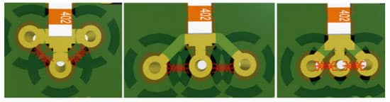
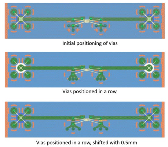
A supporting simulation was also performed using the EMCoS software, which is available for a fee. Among other things, this software must be fed with the exact PCB raw data from the CAD (e.g. Altium). With the help of the EMCoS software, the effect of different positioning of the 3 GND vias was investigated.
In theory, vias with the same electrical potential are expected to form a mutual mutual inductance and thus the total inductance increases the closer they are placed to each other. If the vias are placed at a 90° angle around the GND pad of the MLCCs, they can be connected close to the pad and still result in a large distance between the 3 vias.
SIMULATIONS & MEASUREMENT RESULTS
As expected, the smallest layout (0402) in combination with several vias per GND pad provides the best result due to the smallest ESL. The insertion loss of the bad layout example turns out to be blatantly worse than the rest. Depending on the measurement point, there is a difference of more than 40dB to the next best channel.
If the basic layout rules such as 90° arrangement of MLCCs to ferrite and short pad connection to vias as well as traces are observed, a broadband filter can be successfully designed. The differences in the insertion loss are then only maximum 10 dB depending on the design and via count.
The relatively simple LT Spice simulation can also nicely represent the basic properties of the different measurement channels, although not 100%. The many parasitic properties of the connectors, PCB etc. cannot be easily represented in LTspice.
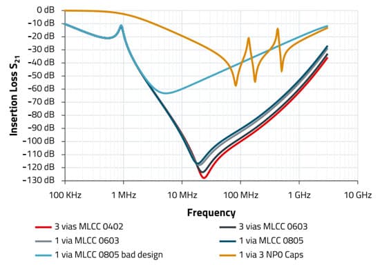

The comparison measurement of the three MLCCs in NP0 and X7R also shows the difference in quality in a practical way.

Although the NP0s achieve better values in the insertion loss at the individual resonant frequencies, the amplitude deflections are also higher in negative form. The NP0 MLCCs generate an LC resonant circuit with higher Q, which in certain frequency regions brings with it the danger of an unwanted amplification of interference components.

SUMMARY
From the differences shown, it can be seen that this PI filter can only work optimally if the textbook layout rules are followed. There are differences of over 40 dB, depending on the frequency in the insertion loss, which in practice can mean the difference between success and failure in the EMC measurement. What has not been considered in this application note is the voltage dependence of the class 2 MLCCs and the DC current dependence of the chip bead ferrite.
These influencing factors mean further differences in insertion loss in practice. If one wants to successfully block supply pins on digital ICs, it is recommended to use several vias per GND pad on the capacitors. In addition, it has been shown that very short stubs to the capacitors and a geometrically unfavorable arrangement also significantly worsen the blocking quality.
The ferrite and the capacitors should be arranged at 90° to each other to avoid unwanted coupling. With the help of the EMCoS simulation it was shown
that GND vias should be placed as far away from each other as possible but always close to the MLCC pad. This way a few dB attenuation can be achieved in the higher frequency range.
The best result was achieved by placing the vias 90° around the GND pad and with a small distance (max. 0.3 mm) to the pad.
The broadband insertion loss without undesired oscillations also shows the enormous advantages of chip bead ferrites over pure capacitor groups. If one nevertheless wants to connect several capacitors in a group, this group should contain a class 2 capacitor (ceramic e.g. X7R) in order to limit the resulting oscillations in amplitude. However, a sufficiently high insertion loss can only be achieved with an additional chip bead ferrite.
Appendix
A.1 Formulas
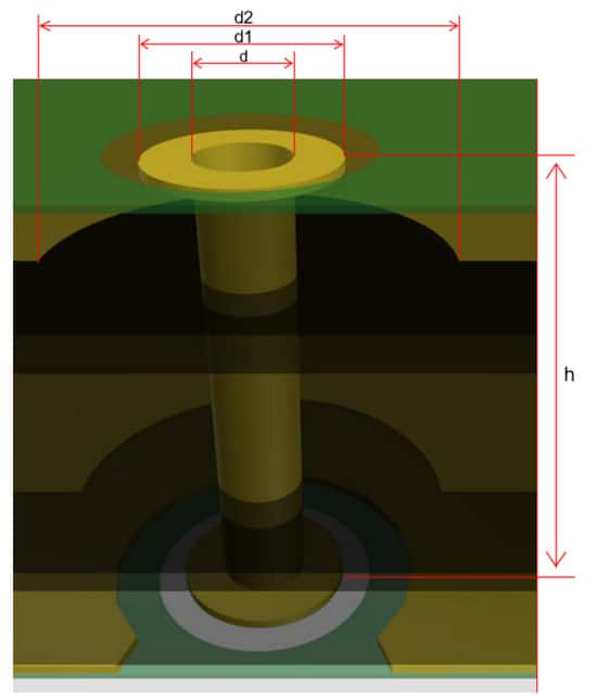
Calculation of parasitic inductance and capacitance of a via:
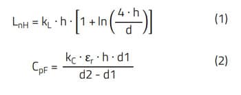
kL = 0.2 nH/mm PCB inductance per unit length
kC = 0.056 pF/mm PCB capacitance per unit length
h = length of the via
d = Via inner diameter
d1 = Via pad outer diameter
d2 = Via clearance diameter on internal layers
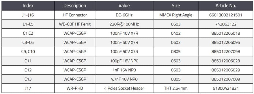
A.2 BOM