

MLCC ceramic capacitors are dominating today’s capacitor market enabling high grade of electronics miniaturization. The continuous downsizing and use of higher and higher dielectric constant materials for MLCC class II capacitors has however resulted in worsening of some electrical parameters stability such as capacitance drop at operating conditions.
Thus, in consequence, what can be considered as an enabling technology for consumer and wearable applications may pose some risk if used in critical applications such as automotive, safety, medical or industrial sector, that are also in need for continuous miniaturization.
Understanding of this behaviour in the worst case application conditions is necessary for reliable designs. In many cases, capacitance loss data available from MLCC manufacturers are given as “typical” performance leaving responsibility for “guaranteed” operation to the electronic system designer. Aim of this article is to explain it basics, provide some guidelines on MLCC class II capacitance loss phenomenon, suggest some design rules & recommendations and initiate discussion within the passive components industry on suitable DC BIAS Capacitance loss reference “guaranteed” conditions.
Key Takeaways
- High‑CV MLCC Class II capacitors can lose most of their nominal capacitance under real operating conditions due to DC bias, AC voltage, temperature and ageing effects acting together.
- Typical manufacturer plots often do not represent worst‑case behaviour, so relying only on simulations can lead to severe under‑capacitance in automotive, medical and industrial designs.
- The effective capacitance can easily drop to a small fraction of the datasheet value; a 10 µF X5R part operated close to its rated voltage may behave like only a few µF in circuit.
- Different vendors and even different part numbers with the same case size and rating can show very different DC‑bias curves and ageing, which complicates second‑sourcing.
- Robust design requires explicit derating, checking DC and AC bias, temperature and ageing together, and validating worst‑case capacitance with measured or guaranteed data, not only typical curves.
- Where the risk or variability is too high, designers should consider larger case sizes, more stable dielectrics or alternative technologies such as tantalum polymer or aluminium hybrid capacitors.
I. Introduction
Chicago Winter Lesson
The Chicago 2019 snow storms and extreme cold weather heavy loaded the local infrastructure and impacted many “unexpected” aspects towards the people everyday lives. There are some warnings and lessons to learn out of this. For example, output from regenerative energy sources solar and wind power was close to zero leaving the existing electric power supply network infrastructure in short supply, not sufficient to meet the peak energy demands.
In electronic sector, the severe weather conditions clearly distinguish between the “good” and “bad” designs of outside environment operating devices. Lips are not moving for a long time at -40C and strong cold wind, so short mobile talk time outside does not hurt so much, nevertheless industrial, safety, infrastructure or automotive systems are required to work reliably, as usual.
We are just entering era of autonomous devices that will have to process more than 4TB of data per day with its sufficient computing power even at Chicago 2019 winter type of weather. It is clear, for example, that sensors and radar electronics directly faced to the outside environment will have to avoid collisions “without excuse” even in such extreme conditions (that under global warming effect may be seen even more often).
There is a clear need for miniaturization in automotive and other “higher reliability” electronics, but copy and paste approach of some “extreme” designs approaches used in consumer electronics may lead to critical failures there. MLCC class II capacitors with typically high level of electrical parameter dependency can be one of the component for attention. Passive component industry has to pick its piece of responsibility to provide assistance and help with correct guidelines, provide alternative solutions, clear design rules and referenced “guaranteed” performance specification.
II. Technical Background
MLCC DC BIAS / AC Voltage & Ageing Capacitance Loss Explained
Ceramic capacitors mostly used in electronics can be split into two main classes of capacitors (see Table 1 and Table 2 below):
- Class I – low loss dielectric capacitors with very stable performance but significantly lower capacitance values (no Cap Loss issue and not the main subject of this article)
- Class II – high dielectric constant but high loss dielectrics

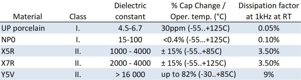

The MLCC class II capacitors are using BaTiO3 ferroelectric materials as a high dielectric constant material to achieve its very high capacitance values in small dimensions. Downside of this material is its strong dependency on operating conditions – namely loss of capacitance – with DC Voltage (DC BIAS), AC Voltage, temperature and ageing with time. In addition, piezo noise may degrade smoothing capabilities of these capacitors at certain condition.
2.1.MLCC Capacitance Ageing with Time
BaTiO3 has a cubic crystal structure above the Curie temperature (approx 125°C or more), but below the Curie temperature it turn into a different crystal structure (tetragonal) that creates a dipole, respectively domains of dipoles with different dipole orientations that reduces its original polarization and thus reduces its capacitance values (spontaneous polarization, no voltage applied). The dielectric grain size/shape/distribution may impact number of dipoles and domains and thus the level of capacitance loss. As this structure changes with time, dielectric constant is reduced and over time, the capacitance will continue to decline.

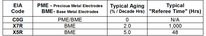

Capacitance Ageing effect depends to MLCC dielectric type and it is constant per time decade (so the process slow down exponentially). Typical values see Table 3 above.
As the capacitance decrease with time and its important to remove some of the other “short term” mechanisms impacts, the reference time for capacitance value reading and its tolerances is set with some time delay.
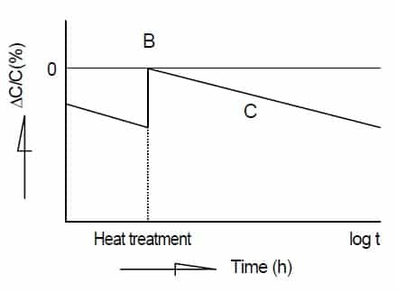
Various manufacturers use different time, but the most common reference points are 48 or 1kHz as also shown in table 3. with note that in reality manufacturers are measuring capacitance with one day or twenty-four hours after “last heat” that is also in accordance to MIL specification conditions. (Re)heating to Curie temperature “reset” the structure and returns capacitance value to its initial value as shown in Fig.1.
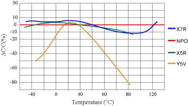
2.2. MLCC Capacitance with Temperature
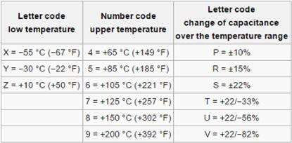
Depending to the dielectric type, capacitance change with temperature – see Fig.2. This is well defined per international standards and even the dielectric class is indicating the temperature stability including its tolerance field as shown in Table 1.

2.3. MLCC Class II Capacitance with DC BIAS
Some of the BaTiO3 dipoles are blocked by DC voltage and it can not move further with small AC voltage changes resulting in loss of capacitance. Capacitance loss due to DC BIAS is the most important contributor for real capacitance value at the operating conditions.
The level of Capacitance loss (number of blocked dipoles) is proportional to the DC field (V/mm), thus capacitor with thinner dielectric and higher volts per dielectric thickness exposure will exhibit higher capacitance loss with DC BIAS. Type and structure of the dielectric (grain size, shape, distribution, impurities) may have also a significant impact to the capacitance loss level.
In consequence, the capacitance loss level may increase with higher CV density (high capacitance in small dimensions) and it may be part number and manufacturer specific. See figure 3. below as an example of 10μF 6.3V MLCC X7R 0805 case capacitance loss with DC BIAS differences between three manufacturers. The loss at rated voltage can vary from -35% to -65% and even at more likely used derated conditions at 3.3V it can be from -12 to -32%, that may result in quite significant in-circuit performance among different manufacturers.

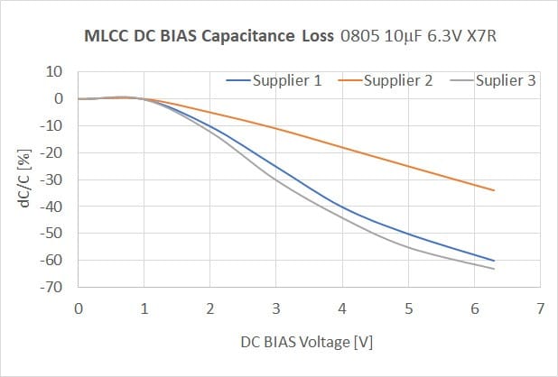
It may be of critical importance to evaluate such characteristics when qualifying alternative MLCC manufacturer under the current tight supply market situation.
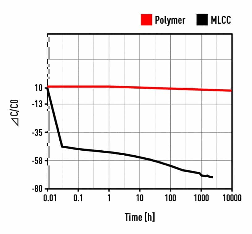
The drop of capacitance due to DC BIAS is not happening immediately, but some time is needed for slower dipoles to be completely blocked. Thus, we can see some fast immediate drop of capacitance at time close to zero after DC Voltage plug in, and some additional drop within tenth of minutes to hour(s) to get to final capacitance drop level. See Figure 4.
Once all dipoles are blocked there is no further significant impact of DC voltage in longer time-frame. The capacitance value still continue to decrease per every decade by spontaneous polarisation as discussed in chapter 1., but this phenomenon is not linked to applied DC voltage. MLCC manufacturers use to talk about behaviour of the capacitor in decades … so what happens in first decade, second decade etc. as this is directly link to physical mechanisms and its impact to overall performance.
Example of the capacitance drop with time can be seen in Figure 4. sourced by Panasonic in their example of tantalum polymer capacitance stability versus MLCC.

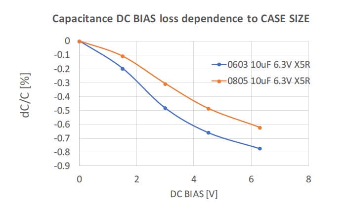
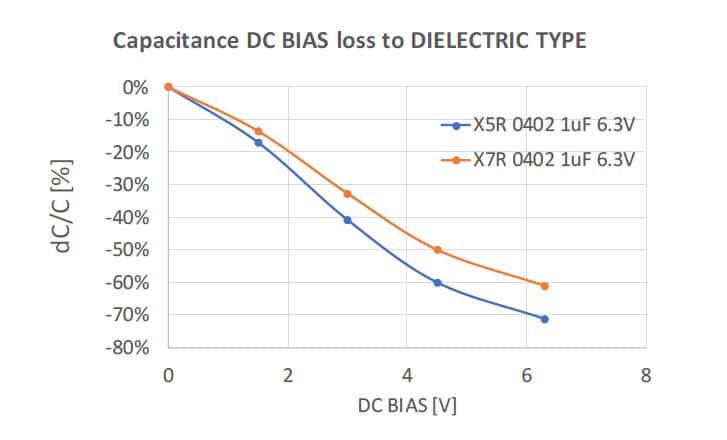
The Capacitance loss with DC BIAS effect can be reduced by using a physically larger case size design that reduces V/mm electrical field exposed to the dielectric. See Fig.5 as an example of capacitance loss with DC BIAS voltage comparison on 10μF 6.3V X5R between 0805 and 0603 case sizes. Another choice, if applicable, is to use a higher grade dielectric type material such as moving from X5R to X7R or X7R to X8R or tighter tolerance field e.g. moving from X7R to X7P types (as per Table 2.). See Fig.6 as an example of capacitance loss with DC BIAS on 1uF 6.3V 0402 capacitor comparison between X5R and X7R types.


2.4. MLCC Class II Capacitance with AC Voltage
Ferroelectric materials (BaTiO3) exhibit some hysteresis in polarization as a function of electric field that is causing MLCC capacitance dependency also to AC voltage. The level depends mainly to the the dielectric type as shown in Figure 7.

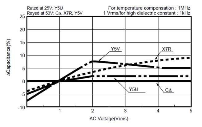
The reference standard capacitor AC volt measure conditions are set to 1Vrms at 1kHz and room temperature. Nevertheless, there are number of MLCC capacitor applications that are operating at significantly lower AC voltage such as 10mV. In this case we can expect capacitance drop of capacitance due to the small AC voltage in range of additional -5 to -15%.
The “AC voltage hysteresis” is also “re-settable” by heating of the capacitor to Curie temperature.
2.5. MLCC piezzo noise
MLCC II BaTiO3 ferroelectric high permittivity dielectric is exhibiting a piezo effect. The Titanium molecule oscillates under external stresses back and forth. Electric signals can mechanically distort the dielectric.

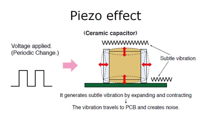
This distortion, or movement, creates a characteristic “buzzing” noise. The effect is used for microphones, piezo sensors etc. but its unwanted for capacitors where it can degrades the signal purity or creates an additional noise. The piezo effect increase with DC BIAS voltage and DC field (v/mm) stress. (thus the parts with highest DC BIAS Cap loss may exhibit also stronger piezo noise). The worst frequency range for piezo effect to happen is between 1 to 10kHz that is typical for example for LED backlight drivers, where use of high CV MLCCs shall be carefully evaluated.
2.6. Summary of MLCC class II capacitance loss behaviour in operating conditions
MLCC class II capacitors are offering very high level of energy density in miniature sizes that is enabling wide range of modern digital devices. On the other hand, the high capacitance density is “compensated” by inferior electrical parameters that may or may not be critical in the specific application area.
There is an multiplication effect of operating conditions that may cause significant loss of capacitance on MLCC Class II capacitors in real application conditions.
for example – if you select a X5R 0805 10uF 6.3V capacitor as 5V coupling capacitor in operating amplifier the capacitor may exhibit (depending to manufacturer):
- -60% drop of capacitance due to DC voltage 5V close to 6.3V maximum rated voltage (as per typical data provided by manufacturer)
- -15% drop of capacitance due to AC voltage being 10mV (as per typical data provided by manufacturer)
- -10% drop of capacitance due to operating temperature (as per specification sheet)
- -5% drop of capacitance each time decade (as per specification sheet)
The total capacitance value at actual condition is then defined as multiplications of the capacitance drop factors.
Cactual = Crated * F DCV drop * F ACV drop * F temp drop * F ageing drop
In example above
Cactual = 10uF * 0.4 * 0.85 * 0.9 * 0.95 = 2.9uF
The actual capacitance value of the 10uF 6.3V MLCC X5R capacitor at the operating condition above is expected to be 2.9 uF.
| Mechanism | Typical reference condition | Typical factor range (example) | Notes |
|---|---|---|---|
| DC bias | VDC as % of rated voltage | 0.3 – 0.7 | Strongest effect; depends on case size, dielectric and manufacturer. |
| AC voltage level | Small‑signal (e.g. 10 mV vs 1 Vrms) | 0.85 – 0.95 | Hysteresis in ferroelectric material reduces capacitance at low VAC. |
| Temperature | Within specified operating temp range | 0.9 – 1.0 | Defined by X5R/X7R/X8R etc.; usually symmetric tolerance band. |
| Ageing (per decade) | Each time decade after last heat reset | 0.95 – 0.98 | Logarithmic decay; dielectric‑type dependent; reset by Curie heating. |
The exact factors are part‑number and vendor‑specific, but this overview helps designers perform quick “back‑of‑the‑envelope” worst‑case estimates before running detailed simulations or measurements.
However, in such operating conditions the real capacitance value can be as low as 10% depending to the specific PN design and manufacturer. Designers of electronic devices has to count with such behaviour and it is always good idea to check the manufacturer datasheets, simulations and its detail specification. Leading MLCC manufacturers are providing sophisticated on-line simulation models, where designers can enter its operating conditions and the software will generate typical plots on the selected part.
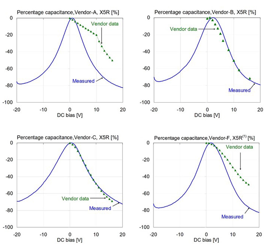
2.7. How trustful are the manufacturers’ simulation data ?
This sub-chapter follows experimental work by I.Novak at col. [2] carried in 2011 on multiple MLCC X5R and X7R vendors.
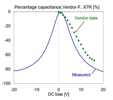
The Figure 7. compare MLCC 1uF 0603 X5R and X7R 16V vendor data with measured data at reference conditions 500 mVrms AC bias at 100 Hz and room temperature.
Not all of the vendors state the conditions (temperature, AC bias, frequency) for their DC bias data, but our 500 mVrms AC bias data seemed to be more likely matching the vendor conditions than the 10 mVrms data set.
Vendor-B and Vendor-C have very good agreement between measured and vendor-predicted capacitance drop. Data for Vendor-A and Vendor-F show bigger differences, and both predictions underestimate the capacitance loss.
As an important note, it has to be add, that manfacturers are continuously improving their software simulation tools and its accuracy. The data presented in Figure 9 are reflecting situation as present in year 2011.


3. How this may impact electronic HW designs
Ceramic capacitors are widely used in today’s electronic circuits. Many of them find applications in power conversion and distribution networks. In high-speed data links they are used as DC-blocking capacitors and occasionally as part of RC terminations. Analog circuits also use them for timing and DC blocking applications.
3.1. Capacitors in power supplies
Power electronic systems require some minimum capacitance value for IC safe operational mode. In case of voltage drop under the cut off value it may result in the power supply mulfunction and critical power loss failures. This very important especially for safet critical applications.
Practical design example – output capacitor in DC/DC converter
Consider a 5 V output rail using a 10 µF, 6.3 V, X5R 0805 MLCC as the only output capacitor of a DC/DC converter.
At this operating point a realistic combination of mechanisms may be: −60% due to DC bias close to rated voltage, −15% due to small‑signal AC, −10% due to temperature and −5% ageing per decade after last heat treatment.
The effective capacitance becomes
Cactual=10µF×0.4×0.85×0.9×0.95≈2.9µF, which is only a small fraction of the nominal value and may compromise control loop stability and hold‑up margin.
In safety‑critical applications, designers should therefore either increase the nominal capacitance, choose a larger case size or more stable dielectric, or switch to an alternative technology such as tantalum polymer or aluminium hybrid to guarantee sufficient capacitance under all conditions.
MLCC X5R or X7R capacitors are favourite choice for many miniature power designs due to its downsizing, low ESR, low ESL and high ripple current capability. However the capacitance loss due to the DC Bias Aging impact may result in significant loss of its capacitance value. The phenomen is dependent on various parameters impacting the internal electrical field strength and thus PN and manufacturer specific.
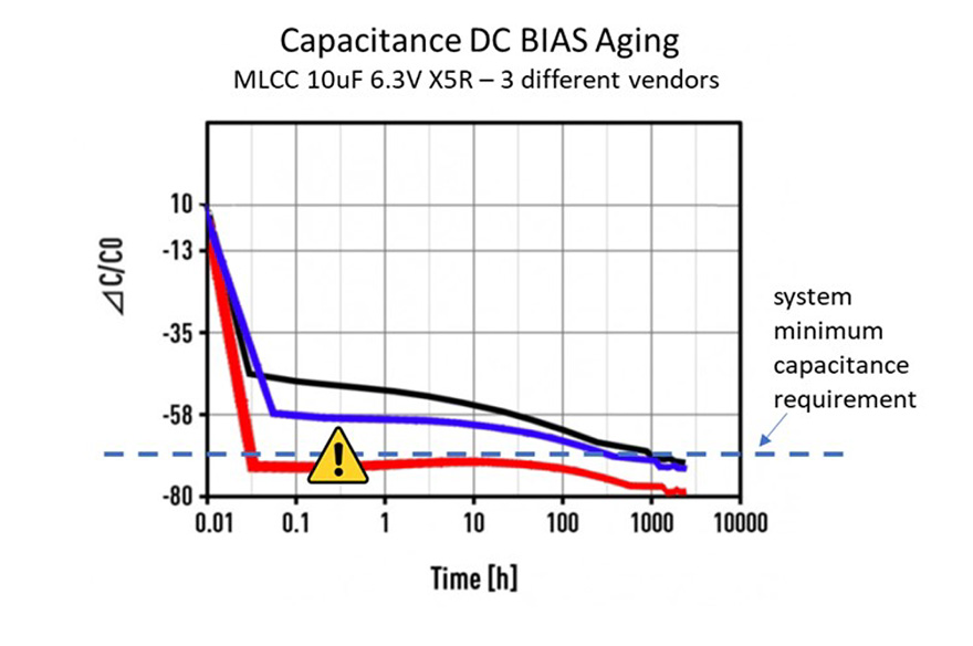
Qualifying a new vendor, using qualified part at different applications conditions without a background knowledge and data can lead to a catastrophic system failures. Figure 10 shows capacitance drop with time example of three different manufacturers of the same PN. Blue and black vendors were originally qualified by the end user, red vendor was add under a risk of line stop due to the MLCC shortage market situation and resulted in system failures.

3.2. Paralleled Capacitors (source:[2])
The application, where the DC and AC bias dependence of MLCCs may need to be taken into account is, when we use MLCCs of different capacitance values in parallel (Figure 11).
If the capacitors are assumed to be ideal, as shown on the left of the figure, all what we need to do is to sum up the different capacitances as they change with DC and AC bias. When their parasitics are also taken into account, the changes of the series and parallel resonances need to be considered as well. The change of capacitances will shift the series and parallel resonances to higher values and Q may also change slightly. If the relative rate of capacitance change is the same for all capacitors, what we get is mainly a shift of the impedance profile to higher frequencies and higher Q at the resonances.


The worst case occurs, when some of the paralleled capacitance decrease, while some others either don’t or actually might increase, perhaps due to the AC bias conditions.
Such a scenario is illustrated with measured data in Figure 12. Two capacitors were parallel connected in the test fixture: a 1uF 0603-size 16V X7R from one vendor and a 47uF 1206-size 6.3V X5R part from other vendor. The minimum around 1 MHz is from the series resonance frequency of the 47uF part. The minimum around 7 MHz is the series resonance frequency of the 1uF part. The peak around 4 MHz is the anti-resonance between the capacitance of the 1uF part and inductance of the 47uF part. Note that all three resonances move towards higher frequencies, indicating that the capacitances of both parts decrease with increasing DC bias.

3.3. Capacitors in LC filters (source: [2])
Probably one of the worst situations is when multiple components joined in the same network, react to DC and AC biases in opposite directions. A typical scenario of this kind is when we use series inductors or ferrite beads for enhanced filtering, followed by shunt capacitors.

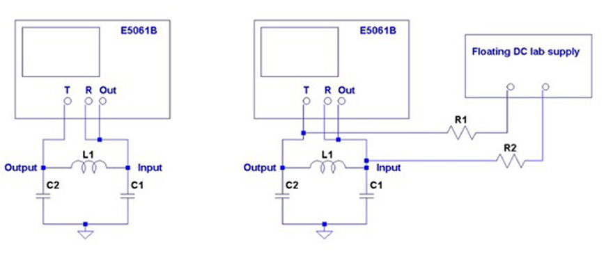
Figure 13: Equivalent schematics of a PI filter with series ferrite element and parallel MLCC at the output. Left: setup with no DC current bias through L1. Right: setup with DC current bias through L1.
If this filter circuit has to handle substantial DC current and the inductive element is not properly sized, its inductance may drop due to the DC current flowing through the part. If at the same time the filtered DC voltage reduces the capacitance of the MLCC part at the output of the filter, we end up with reduced inductance and reduced capacitance, resulting in a significant shift of the filter’s cutoff frequency. This effect was tested with the circuit shown in Figure 13.
The circuit under test was a simple PI filter, composed of two bypass capacitors and a series ferrite bead. The C1 capacitor on the input side of the filter was a 390uF 16V electrolytic type bulk capacitor with little or no DC and AC bias dependence to mimic a low value of input feed impedance. The C2 capacitor on the output was a 47uF 6.3V X5R 1206-size MLCC. The L1 series element was a commercially available ferrite bead, rated for 2A maximum current.

Figure 14: The two plots show the cumulative transfer responses of the circuit from Fig.11. Left plot: bias range limited to 0-4V and 0-1A. Right plot: bias range is 0-16V and 0-1.5A.
The plot in Figure 14 show all the measured data traces. The plot on the left has the DC bias voltage and current limited to the reasonable ranges of 0-4V and 0-1A, respectively. The 4V and 1A DC bias limits are 63% and 50% of the rated 6.3V and 2A limits, respectively.
There are two ranges marked on the plot along the two axes: the range of transfer-function magnitude variation at 260 kHz is 50 dB; the range of frequency variation at the -50 dB level is approximately 3.2 : 1. The plot on the right shows all traces for the full measured 0-16V bias voltage and 0-1.5A bias current ranges. There are two ranges marked on this plot, too: at 260 kHz the transfer-function magnitude variation is 68 dB; the range of frequency variation at the -50 dB level is approximately 7.2 : 1.
4. How to measure capacitance with BIAS in mass volume
The obvious task from designers is to get the worst case MLCC class II capacitance drop at referenced conditions as the basic for their design considerations. As mentioned in previous chapters, manufacturers are continuously improving ther simulation online tools, where typical plots at operating conditions can be simulated to provide information of the capacitor behaviour at the required environment.
The online simulation tools may be sufficient for many kind of consumer electronics operating at standard environment. Nevertheless, mission critical system designers can not rely on „typical“ data plots and requiry 100% „guaranteed“ point of the capacitance value. Interest to use high CV MLCC in safety automotive, defence or medical system is increasing under the continuous electronics miniaturisation requirements.
Manufacturers, on the other hand, can guarantee only what they can 100% measure in mass manufacturing.
There are two general ways how to measure Capacitance with DC BIAS: Direct and Indirect capacitance measurement.
4.1. Direct capacitance measurement
The direct measurement that is used today in mass manufacturing by most of MLCC manufacturers is based on LCR bridge measure meters build into a 100% electrical parameter testers. The bridges, contacting systems and el.tester design must ensure the appropriate test accuracy, speed, reliability and lifetime to be able to measure high quantity of the manufactured MLCC capacitors of all kinds and sizes.
Typical LCR bridges used by el.tester manufactures is a class of HP4263B measure bridges (Fig.15) that are used to measure Capacitance, Impedance, DF or ESR values at frequencies from 100Hz to 1MHz.


Figure 15. HP4263B LCR measure bridge
While measure parameters of the bridge are satisfying needs for electrical parameters fast and reliable measurement, the DC BIAS conditions are limited to maximum 2V. This comply to standard capacitance reference conditions: Frequency 1kHz or 120Hz AC Voltage: 0.5 or 1.1V AC volt and BIAS of 2V DC.
The LCR bridges can also accept some level of external BIAS, but mostly the value is limited. In case the HP4263B bridge the maximum BIAS level is just 2.5V. More expensive bridges can operate with higher external voltages, but often limited to 50V maximum.
Additional factor that complicates Capacitance with higher DC BIAS measurement is a charging time. Depanding to the capacitance value of the measured part, some time constant delay has to be applied before measurement to allow capacitor to be fully charged. This may be other complication for adoption of capacitance measurement at el.tester as there may be only few (tenth)milliseconds time slot for the measurement not to reduce the tester speed and throughput significantly.
4.2. Indirect (transient) capacitance measurement
Capacitor charging and discharging characteristics are depending to its capacitance value. Charging current is following the basic equation:

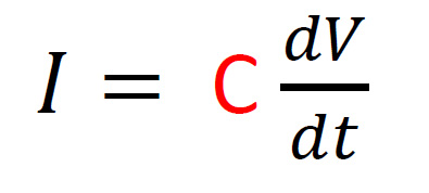
where, I = charging current; dV/dt = voltage increase; C = capacitance
Thus in case of stable voltage increase dV/dt capacitance value can be calculated based on the measured current value.

The indirect capacitance method during transient as shown in Figure 16 can be theoretically applicable during measurement of leakage current at rated voltage that is usually part of todays MLCC capacitors 100% electrical measurements in mass production.
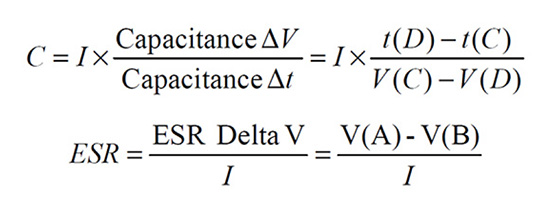
Capacitance (and ESR) values can be also evaluated from a discharging characteristics as shown in Figure 17. [3]

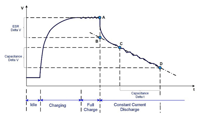
Under the constant discharging current, the Capacitance and ESR values can be calculated from equations:

The main challenge of the indirect capacitance measurement here would be to evaluate its correlation to the Capacitance versus DC BIAS characteristics applicable to wide range of types and case sizes. Also cost for electrical tester modifications may be of consideration for realistic implementation into mass manufacturing.
FAQ
MLCC DC bias capacitance loss is the reduction of effective capacitance when a DC voltage is applied to Class II ceramic capacitors, caused by blocking of ferroelectric dipoles in the BaTiO3 dielectric. This effect is strongest for high‑CV parts in small case sizes and increases with higher electric field (V per dielectric thickness).
In automotive, medical, industrial and telecom systems the minimum capacitance is often safety‑critical, so a capacitor that drops to a fraction of its nominal value can cause power rail instability, loss of filtering or even system failure. High‑CV MLCCs can easily lose more than half of their capacitance under real operating conditions, which is unacceptable without proper derating and validation.
The main mechanisms are DC bias, AC voltage amplitude, temperature characteristics of the dielectric and logarithmic ageing over time after the last Curie‑temperature heat treatment. In practice these factors multiply, so the real capacitance in circuit can be much lower than suggested by a single DC bias curve.
Yes, parts with the same case size, voltage rating and nominal capacitance from different vendors can show very different DC bias and ageing curves. Measurements on 10 µF 6.3 V X7R 0805 parts showed losses at rated voltage ranging roughly from −35% to −65%, which heavily impacts second‑sourcing and risk assessments.
Vendor simulation tools are useful, but historical measurements show that some manufacturers significantly underestimated capacitance loss compared to measured data, while others matched very well. Designers should therefore treat simulations as typical behaviour and still verify worst‑case performance with measurements or guaranteed specification points.
Effective measures include using larger case sizes to reduce electric field, choosing more stable dielectrics (for example X7R instead of X5R), derating voltage, and using multiple capacitors in parallel with margin. When MLCC behaviour is still too variable, alternative technologies such as tantalum polymer or aluminium hybrid capacitors can provide more stable capacitance over voltage, temperature and time.
A practical approach is to define at least one guaranteed capacitance loss limit at a specified percentage of rated voltage, measured under clear reference conditions (post‑deageing, room temperature, specified AC test voltage and DC bias duration). This gives designers a fixed worst‑case point for calculations while allowing manufacturers to optimize their production around that requirement.
SUMMARY & CONCLUSION
- Over the past years, multi-layer ceramic capacitors have undergone significant improvements. The volumetric density has increased several folds. This unfortunately resulted in a big increase in DC and AC bias sensitivity for many parts. In particular, X5R and X7R parts, which previously showed only modest bias dependence, exhibit significant capacitance drops.
- The increased bias dependence creates additional challenges for users during the design and validation phase, and increases design complexity, since filters with otherwise identical filtering requirement now may require different component selection if they need to work in different bias environments.
- To help the users, all major vendors today supply at least DC bias information with their MLCC parts and simulation tools under continuous improvement in complexity and accuracy.
- Nevertheless, so far the capacitance versus BIAS data available from manufactures are based on typical characteristics as 100% mass production volume capacitance under the high DC BIAS measurement present a considerable technical and economical challenge for MLCC manufacturers.
Specification Guidelines
Future procurement specification, in ideal case, would define at least one point of the Capacitance versus DC BIAS characteristics that could be “guaranteed” for the selected part.
Procurement specification proposal to be agreed between customer and supplier:
A typical internal specification or drawing could use wording similar to: “Capacitance loss at 100% of rated voltage shall not exceed −70% at reference test conditions (post‑deageing, room temperature, 1 kHz, 1 Vrms, DC bias applied for at least 10 h).”
Such a single guaranteed operating point allows the design team to calculate worst‑case effective capacitance for their actual bias, temperature and ageing profile while the supplier remains responsible for manufacturability and statistical variation around that point.
Capacitance loss guaranteed not to exceed XX% (for example -70%)1 at 100%2 of rated voltage, measured at reference conditions: after 12hrs3 post last de-ageing and DC BIAS voltage applied at least for 10hrs4 at RT, 1kHz and 1VAC.
The supplier shall also provide typical Capacitance loss with DC-BIAS Ageing charts or link to an on-line simulation tool. Additionally to the graphs the supplier shall provide a tolerance band for the graphs which can be guaranteed by the supplier. Such specification would help designers to see some fixed capacitance loss guaranteed working point and evaluate the worst case at the edge operating conditions.
Customer Designer Guidelines:
If you discover that a particular capacitor is unsuitable due to capacitance loss as defined in the specification above, you have the following options:
- You can check if lower Capacitance DC loss / piezo suppression series is available by a manufacturer (need check with purchasing team as this can be more expensive part or single source)
- Use a larger capacitance value so that when the capacitance loss is considered, you still have enough capacitance for the required functionality. Note: higher values may have even worse DC bias characteristics due to even higher CV factor. This also may be an issue of distortion in large-signal AC, and likely will just make the problem worse and may not lead to the problem solving.
- Use a physically larger package size. This would reduce V/mm electrical stress and thus reduces also DC BIAS capacitance loss dependency. So, if you have enough room in your design, moving one step up in case size, for example from 0402 to 0603, 0603 to 0805 or a 1210 will significantly reduce the issue.
- If applicable you can consider using more stable dielectric type such as moving from X5R to X7R, from X7R to X8R dielectric type or tighter tolerance field such as from X7R to X7P types. (multi-sourcing and price increase options to be checked)
- Use a different capacitor type. Sometimes, you won’t be able to escape the DC bias issue or piezo issues at all. In this case, consider looking at a different capacitor type, such as an aluminum hybrid if you have enough board space or a tantalum polymer capacitor that may provide low profile, high CV and stable option.
Notes:
- The level of defined maximum capacitance loss may be a part number specific, the actual value or some more detail guideline, if possible, to introduce some general rules to be discussed with manufacturers.
- The cap loss reference DC BIAS is suggested to 100% of rated voltage, but it can be changed upon discussion with manufacturers.
- 12 or 24hrs measurement after last heat/deaging is a standard time used also in MIL standards to define state of the dielectric after the last “reset”.
- 10hours of DC applied as reference selected in respect to decades behaviour references that is used by MLCC manufacturers … what is happening in first, second, third decade …etc. 1hour may not be sufficient in some cases to see all slow polarization to happen and need to add some safety, thus 10hours (or more) is set as the reference point.
How to design reliably with MLCC Class II capacitors under DC bias
- Step 1 Identify critical nodes and required minimum capacitance.
Describe which rails, filters or timing networks are safety‑relevant and document the minimum effective capacitance needed over voltage, temperature and product lifetime, not just the nominal value.
- Step 2 Estimate worst‑case capacitance using derating factors.
Apply multiplicative factors for DC bias, AC voltage, temperature and ageing using vendor data or typical ranges (for example 0.3–0.7 for DC bias, 0.85–0.95 for low AC, 0.9–1.0 for temperature and 0.95–0.98 per time decade for ageing).
- Step 3 Check vendor curves and simulation tools.
Use manufacturer DC bias and AC bias plots or online tools for the exact part number to refine your calculation, keeping in mind that many tools represent typical rather than worst‑case behaviour.
- Step 4 Adjust MLCC type, size and value.
If the effective capacitance is too low, iterate on dielectric type, case size and nominal capacitance and consider using multiple capacitors in parallel to restore margin at operating conditions.
- Step 5 Consider alternative capacitor technologies.
When MLCC behaviour remains too variable or piezo noise is unacceptable, evaluate MLCC class I. solution (compare effective capacitance of the selected MLCC class II with MLCC class I stable dielectrics), tantalum polymer or aluminium hybrid capacitors, which offer more stable capacitance versus voltage and time at the cost of larger size.
- Step 6 Define a clear capacitance‑with‑bias requirement in specifications.
Include at least one guaranteed capacitance loss limit at a defined percentage of rated voltage and reference conditions in the procurement specification or internal drawing to align expectations with suppliers.
- Step 7 Validate the final design with measurements.
Measure capacitance under representative DC and AC bias, temperature and ageing conditions (or accelerated equivalents) on real hardware to confirm that the effective capacitance stays above the required minimum throughout the product life.
Reference
- MLCC Capacitors Explained; Kemet Webinar Video
Available at: MLCC Capacitors Explained; Kemet Webinar Video - How to Read MLCC Spec Sheet? Samsung Video
Available at: How to Read MLCC Spec Sheet? Samsung Video - MLCC Class II DC BIAS Explained, Samsung Video
Available at: MLCC Class II DC BIAS Explained, Samsung Video - MLCC Ageing; Samsung Video
Available at: MLCC Ageing; Samsung Video - How to determine and measure MLCC ripple current and ESR
Available at: How to determine and measure MLCC ripple current and ESR - Resonant OBC Capacitors
Available at: Resonant OBC Capacitors - Tantalum and Niobium Capacitors
Available at: Tantalum and Niobium Capacitors - Tantalum Polymer use in GaN based applications
Available at: Tantalum Polymer use in GaN based applications - Tantalum Polymer vs Aluminum Polymer Capacitors in Miniature Switching Power Supplies
Available at: Tantalum Polymer vs Aluminum Polymer Capacitors in Miniature Switching Power Supplies - Conductive Polymer Capacitor Market and Design‑In Guide to 2035
Available at: Conductive Polymer Capacitor Market and Design‑In Guide to 2035 - I.Novak et col.; “DC and AC Bias Dependence of MLCC Capacitors Including Temperature Dependence”; DesignCon East 2011; http://electrical-integrity.com. Re-published under author’s permission on passive-components.eu website.
- Capacitances of Nonlinear MLCCs: What Datasheets Don’t Tell You
This article can be downloaded in pdf version here.

