
Following EPCI initiative on MLCC DC BIAS issues investigation that is discussed during the PCNS 2019 symposium here, EPCI is pleased to get author’s permission to publish a paper written by Istvan Novak and col. about a real measurement on MLCC DC BIAS effect. Istvan Novak and his team in this paper measured characteristics on several different MLCC ceramic capacitors and compared their performance, including the effect of temperature. It will also be shown how the same nominal part from different vendors may behave very differently and also how some X7R capacitors may behave the same or even worse than X5R parts. The impact of measurement conditions, for instance preconditioning and/or dwell time, will be considered as well.
Original paper published at DesignCon East 2011 conference can be downloaded in pdf from Electrical Integrity web page here.
Abstract
The capacitance of certain capacitors depends not only on the chosen dielectric material, geometry and temperature, but also on the DC and AC bias applied to the part. Some ceramic capacitors with high volumetric density today exhibit a strong dependence on the DC and AC bias. To achieve high capacitance values, the initial dielectric constant of the ceramic material is raised to the highest practical values and at the same time the thickness of individual dielectric layers is minimized. The dielectric constant and the capacitance change as the operating point moves around the hysteretic curve due to the AC and DC bias. Recent advances reduced the layer thickness to the single-digit micrometer level and it pushes the problem into material categories, such as X5R and X7R, which previously showed much less bias dependence. This paper will show measured characteristics on several different MLCC devices and compare their performance in this respect, including the effect of temperature. It will also be shown how the same nominal part from different vendors may behave very differently and also how some X7R capacitors may behave the same or even worse than X5R parts. The impact of measurement conditions, for instance preconditioning and/or dwell time, will be considered as well.
I. Introduction and background
It has been long known in the industry that the capacitance of multi-layer ceramic capacitors with ferroelectric dielectric materials depends on DC and AC bias. Years ago parts with Class II ceramics (with an allowed +-15% or less capacitance variation in the specified temperature range) exhibited a modest 20 to 40% maximum capacitance degradation over the full DC working range, and only Class III ceramics (with an allowed capacitance variation of +-22% or more in the specified temperature range) came with a maximum capacitance loss of 60% or higher. Figure 1 shows such an illustration from a vendor catalog.
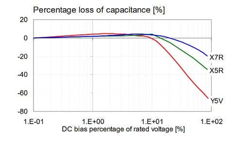
Figure 1: Typical DC bias dependence from the past for three different MLCC types. Data from Figure 8 of [1].
Today, however, actual vendor data often shows a much more dramatic loss of capacitance even for Class II parts. To increase the capacitance of an MLCCs in a given case size (with fixed L, W and H), capacitor vendors have two basic options: improve the material to achieve higher εr, or increase the number of dielectric layers (N) by making the dielectric layers (th) and/or the conductive layers thinner. Ferroelectric materials, such as ceramics, have high εr, but as εr increases, they come with a price of increased sensitivity to temperature and bias. At the same time, if we increase the number of layers by reducing th, a given voltage across the capacitor terminals will create a higher field strength (bias) across the dielectric layers.
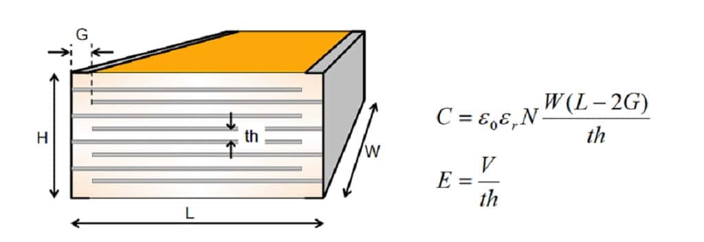
Figure 2: MLCC construction and the approximate calculation of capacitance. N is the number of dielectric layers in the capacitor. V is the voltage applied across the capacitor, E is the field strength across each dielectric layer.
Dielectric materials for MLCCs come in three categories. Class I materials (for COG and NPO parts) are very stable, but can achieve only low εr. Class II materials have been the sweet spot for a long time, offering a compromise between moderately high dielectric constant and reasonable stability. Class III materials have very high dielectric constant, but also exhibit high instability. The most typical Class II categories are X5R and X7R. Both have a maximum of +-15% allowed change of capacitance with temperature in the temperature range of -55 to +85 and +125 degC, respectively, for X5R and X7R. Ferroelectric materials, similar to ferromagnetic materials, exhibit a hysteretic response to excitation. The classic and detailed theory can be found for instance in [2]; a more contemporary summary can be found in [3].
II. Scope of work
From each vendor, multilayer ceramic capacitors come in many different capacitance values, tolerances, rated voltages, case sizes, package styles and temperature characteristics. The number of available different models is so huge that it made no sense to attempt a systematic study on the entire offering. To limit the permutations, a few characteristics have been identified and sampled across some of the major vendors. It is still the common understanding that Class I ceramics have very little or no DC and AC bias dependence and therefore they were not included in the study.
Similarly, Class III (and Class IV, which are now considered obsolete) capacitors, known to have very poor stability and large DC and AC bias sensitivity, were also excluded from the study. From Class II ceramics two temperature characteristics, X5R and X7R were selected, primarily because earlier these capacitors showed relatively modest bias dependence, and also it was a common assumption that X7R capacitors had less bias dependence than their X5R counterparts (assuming everything else being the same).
Altogether more than two dozen different capacitor models were tested from six different MLCC vendors. For reference purposes, one electrolytic and one polymer tantalum capacitor model was also tested, all others were MLCCs. The six vendors are identified by letters A through F. To further limit the number of parts, MLCC bodies were limited to 0402, 0603, 0805, 1206 and 1210 sizes and the rated voltage of parts was limited to the 4 to 16V range.
To get a feel about vendor dependence of bias sensitivity, some capacitors having the same nominal specifications were obtained from multiple vendors. Some other capacitors were compared from the same vendor with X5R versus X7R temperature characteristics, with capacitances, case sizes and voltage ratings being the same.
III. Instrumentation setup
The instrumentation is shown in Figure 3 [4]. Scripts were developed to control the instrument and to step through pre-defined ranges of DC bias voltages, while the AC bias was kept constant as described in [4]. At any given AC bias level the DC bias wasstepped in increments of 1% of the rated voltage, and the impedance profile was measured at 201 frequency points in the 100 Hz to 10 MHz frequency range. The scripts allowed for different ways of stepping through the DC bias voltages: sequential monotonic, return to zero and also alternating positive and negative values starting with maximum, approaching zero. Separate parameters of the scripts took data points at user-defined times after changing bias conditions. Most parts were measured multiple times for at least 100 seconds after each change in the bias setting, resulting in a six-to-ten hours of total measurement time at each AC bias level.
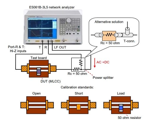
Figure 3: Instrumentation setup for measuring DC and AC bias sensitivity of MLCCs.
Most measurements in this study were carried out at room temperature only; temperature dependencies are shown at the end of Section IV. During the measurements data was recorded on the built-in hard disk of the instrument and separate scripts were used to read the files and put together the data pieces in various forms, for instance showing the capacitance on 3D plots as a function of DC bias voltage and frequency.
IV. Measurement results
This section gives a summary of various measurement results.
Unit-to-unit variations
Unit-to-unit variation is illustrated with the DC bias sensitivity measured on ten samples of 1uF 0603 16V X5R parts from Vendor-F (see Table 1). The data is plotted in Figure 4. When we remove the initial capacitance tolerance, the percentage capacitance loss shows a tight distribution. This was found to be typical on all of the measured samples, which confirms that variations seen among parts from different vendors is characteristic to the particular vendor’s materials and processes rather than random part-to-part variations.
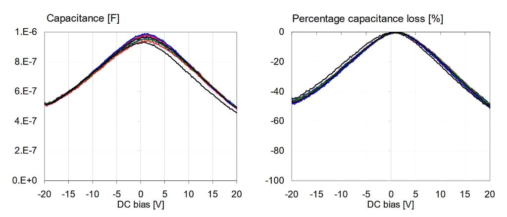
Figure 4: Distribution of DC bias dependence across ten samples of 1uF X5R 0603-size 16V parts from the same vendor.
Comparing DC bias sensitivity of X5R and X7R parts
To test the prevailing assumption that X7R parts may inherently have lower bias sensitivity than comparable X5R parts, various groups of parts were measured. In each group there were X5R and X7R parts from different vendors, but all other specifications were the same. One such group is summarized in Table 1. The group consisted of eight different models of 1uF 0603-size 16V MLCC part numbers from five different vendors. Five models were X5R rated, three of them were X7R. Vendor-F had two different X5R part numbers with different bias sensitivity. Today a 1 uF 16V part in 0603 size is not considered high density, and therefore with these parts we can test the assumptions that X7R parts might have lower DC bias sensitivity.
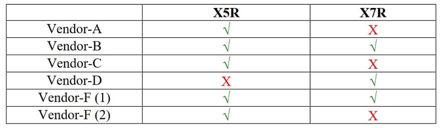
Table 1: Vendor allocation for comparing X5R and X7R 1uF 0603 16V parts.
The parts were measured with two constant AC bias levels: 10 mVrms and 500 mVrms. The DC bias was stepped through sequentially in 0.2V increments from -20V to +20V. The data shown here were readings taken 100 seconds after each change in the bias conditions. Figure 5 shows the overall picture, including all eight parts.
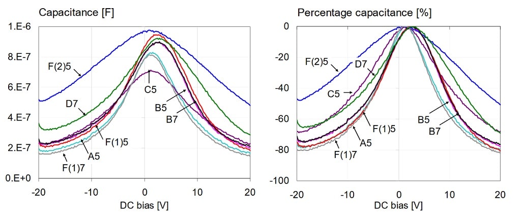
Figure 5: Overall capacitance versus bias for all 1uF 0603 16V models, measured at 100 Hz and 10 mV AC bias. Left: absolute capacitance. Right: percentage capacitance compared to the maximum value.
Figure 6 compares the percentage capacitance change separately for the X5R and X7R parts.
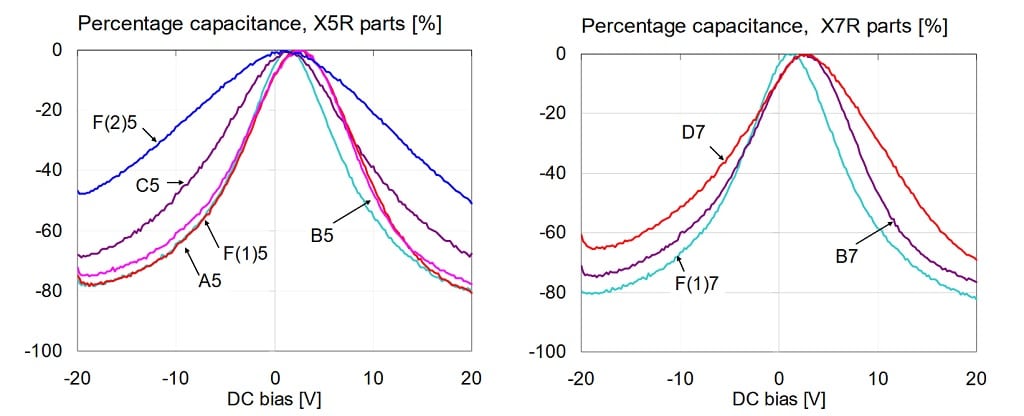
Figure 6: Percentage capacitance versus bias for 1uF 0603 16V models, measured at 100 Hz and 10 mV AC bias. Left: X5R parts. Right: X7R parts.
Two of the vendors had both X5R and X7R parts in the mix. Figure 7 compares the X5R and X7R parts for each of these vendors.
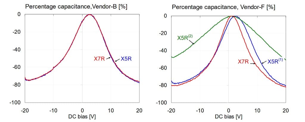
Figure 7: Comparison of percentage capacitance versus bias for 1uF 0603 16V models, measured at 100 Hz and 10 mV AC bias. X5R and X7R parts from Vendor-B (on the left) and from Vendor-F (on the right).
Note that there was no measurable difference between the X5R and X7R parts from Vendor-B. Note also that the X5R and X7R parts from Vendor-F showed the opposite of the expected result: the X7R part being more sensitive then the X5R parts. The same tests were also repeated with 500mVrms AC bias. Figures 8, 9 and 10 show the results. First Figure 8 shows the overall comparison for all parts.
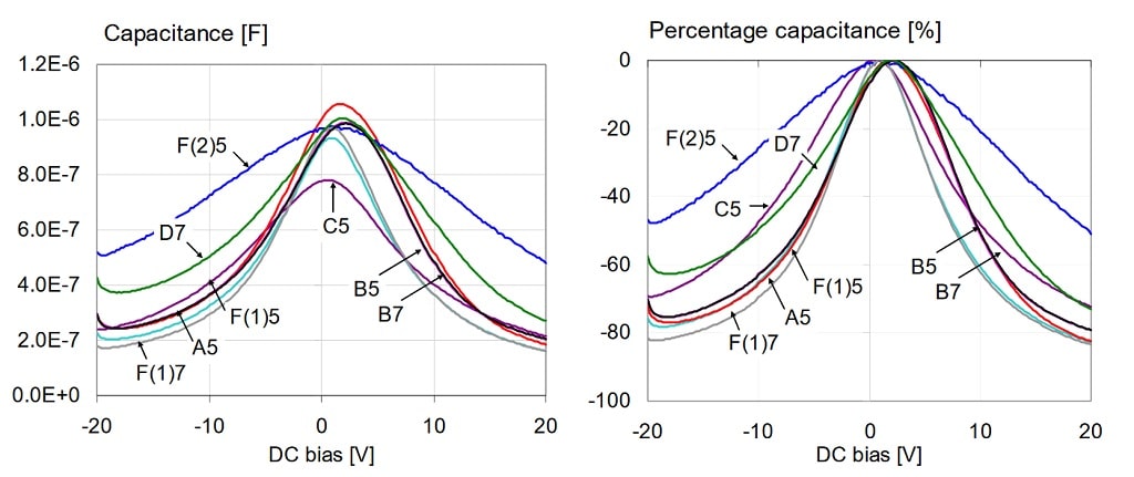
Figure 8: Overall capacitance versus bias for all 1uF 0603 16V models, measured at 100 Hz and 500 mV AC bias. Left: absolute capacitance. Right: percentage capacitance compared to the maximum value.
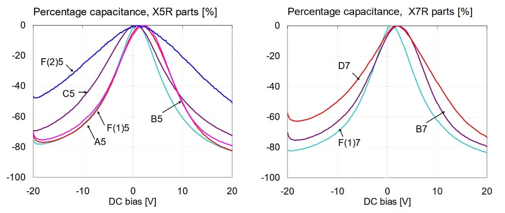
Figure 9: Percentage capacitance versus bias for 1uF 0603 16V models, measured at 100 Hz and 500 mV AC bias. Left: X5R parts. Right: X7R parts.
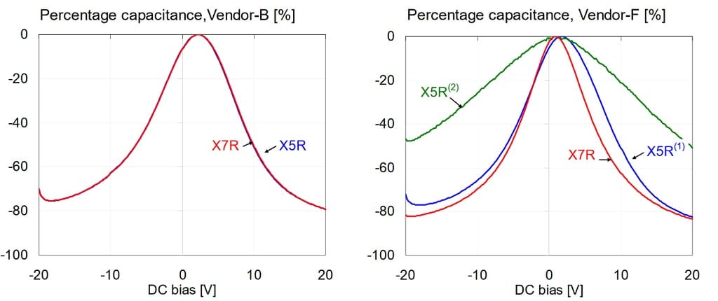
Figure 10: Comparison of percentage capacitance versus bias for 1uF 0603 16V models, measured at 100 Hz and 500 mV AC bias. X5R and X7R parts from Vendor-B (on the left) and from Vendor-F (on the right).
The trends and observations are the same that we had for the 10 mV AC bias case. The only difference is that the absolute capacitance is now higher for all parts. We will look into this later when we do the AC bias sweep.
All of the vendors included in this study have some amount of bias dependence data publicly available on their websites. Vendors A and F have downloadable executable files with the relevant data included in the data base. Vendors B, C and D offer online tools. All of these vendors have DC bias dependence information; some also have AC bias data.
The following figures compare vendor data with our measured data at 500 mVrms AC bias at 100 Hz and room temperature. Not all of the vendors state the conditions (temperature, AC bias, frequency) for their DC bias data, but our 500 mVrms AC bias data seemed to be more likely matching the vendor conditions than the 10 mVrms data set. Figures 11 and 12 compare each part in the X5R and X7R groups, respectively. Note that Vendor-B and Vendor-C have very good agreement between measured and vendor-predicted capacitance drop. Data for Vendor-A and Vendor-F show bigger differences, and both predictions underestimate the capacitance loss.
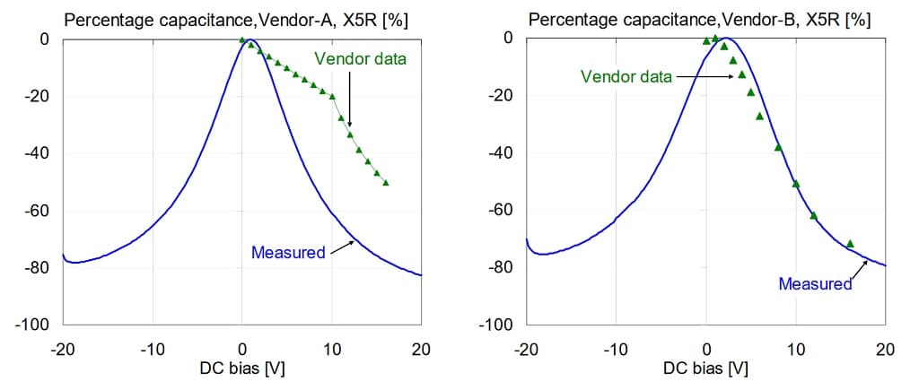
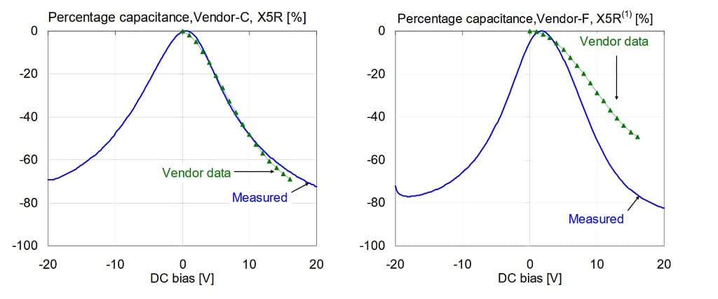
Figure 11: Comparison of percentage capacitance versus bias for 1uF 0603 X5R 16V models, measured at 100 Hz and 500 mV AC bias. On all plots green triangle markers indicate vendor data; solid blue line shows our measured data.
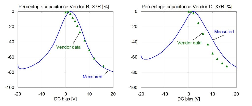
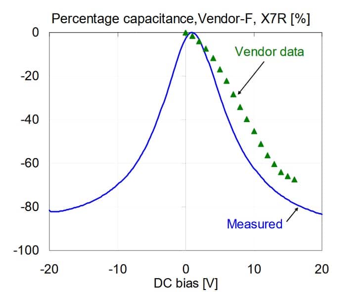
Figure 12: Comparison of percentage capacitance versus bias for 1uF 0603 X7R 16V models, measured at 100 Hz and 500 mV AC bias. On all plots green triangle markers indicate vendor data; solid blue line shows our measured data.
Note that from Vendor-B not only the measured DC bias data matches closely between X5R and X7R parts, but the vendor bias information is also completely the same for the two parts. This again suggests that this vendor may use the same part (or at least the same dielectric composition and layer thickness) for these parts with X5R and X7R specifications. Similarly, vendor data from Vendor-F confirmed the measurement results that the X7R parts have higher DC bias sensitivity then their X5R parts.
ESR and ESL variation with DC bias
It is reasonable to assume that ESR and ESL do not change noticeably due to DC bias. Measured data supports the assumption for ESL and also for ESR at and above the part’s SRF. Below SRF, however, ESR changes proportionally to the capacitance change. This happens because below SRF the loss is dominated by the parallel dielectric loss. For the same loss tangent lower capacitance means smaller parallel conductance, which is transformed into higher resistance in the series equivalent circuit.
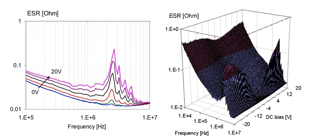
Figure 13: ESR of a 1uF 0603-size X5R 16V part. Line plot on the left, 3D plot on the right.
Figure 13 plots the measured ESR as a function of DC bias. Note that at and above SRF the ESR does not change with DC bias. There are increasing peaks somewhat below SRF with increasing bias: this is the manifestation of piezoelectric effects.
Beware of details
In volume manufacturing, having alternate sources for the components is an important requirement. When selecting alternate sources, we need to determine which parts are considered interchangeable. One might think that if the alternate part comes in a body with identical footprint but lower height, it would satisfy the requirements.

Figure 14: Percentage capacitance versus bias for three 1uF 0603 16V models. Data is predicted by Vendor-C.
Figure 14 illustrates a situation, where this may not work. In the X5R vs. X7R comparison above, from Vendor-C we had an X5R part in a 0.8mm tall package. To compare apples to apples, we made sure that all other parts in the comparison mix had the same 0.8mm nominal package height. However, Vendor-C for instance also offers other variants of 1uF 16V 0603 parts: an X5R part with 0.5mm nominal height and an X7R part with 0.8mm nominal height. Figure 14 shows the DC bias dependence of capacitance for these three parts, predicted by the vendor’s data base. Note that the 0.5mm tall X5R component, possibly due to having thinner dielectric layers, has substantially more capacitance loss for the same bias voltage.
AC bias dependence
The capacitance is also dependent on the AC bias level. To show this in more detail, several parts were measured sequentially with different fixed AC bias levels.
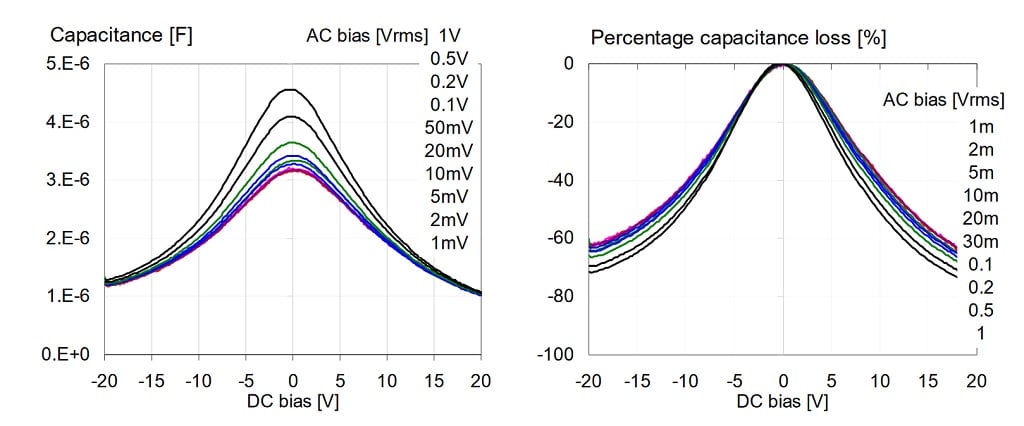

Figure 15: AC bias dependence of a 4.7uF 0805-size 16V X5R sample from Vendor-F. Top left: absolute capacitance at 100 Hz. Top right: percentage capacitance loss. Bottom: absolute capacitance as a function of AC bias, with DC bias as parameter. On all plots the bias parameter is listed in the order of the traces.
Figure 15 shows the data for a 4.7uF 0805-size 16V X5R part from Vendor-F. Note that the capacitance does not change much until the AC bias get above 50 mVrms. The AC bias dependence is the biggest with 0 DC bias, and becomes very small as DC bias approaches the nominal rated voltage.
Dependence on timing and sweep type
After applying bias, we can observe an immediate jump in capacitance, followed by a slower relaxation. One might expect that parts exhibiting higher initial jump will also exhibit more relaxation, but this is not necessarily the case. We illustrate this on two parts: Part-1 is from Vendor-A, a 47uF 1206-size 6.3V X5R part; Part-2 is from Vendor-D, a 4.7uF 0805-size 16V X7R part. Plots in Figure 16 show the capacitance measured at room temperature, 100 Hz frequency and 10 mVrms AC bias. Readings were taken from swept-frequency measurements; one sweep took 9.5 seconds. Part-2 showed slower decay and therefore a longer test period of over 150 seconds was applied. Between each step in the DC bias, the parts were brought down to zero bias.
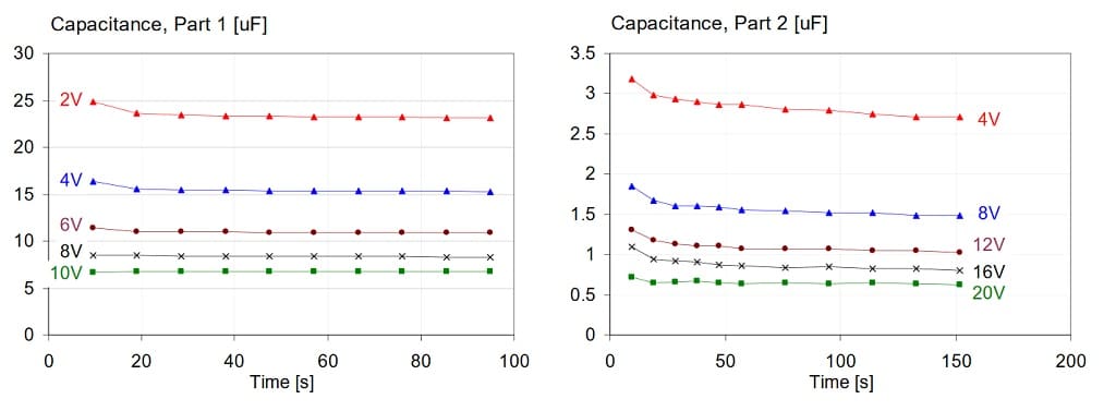
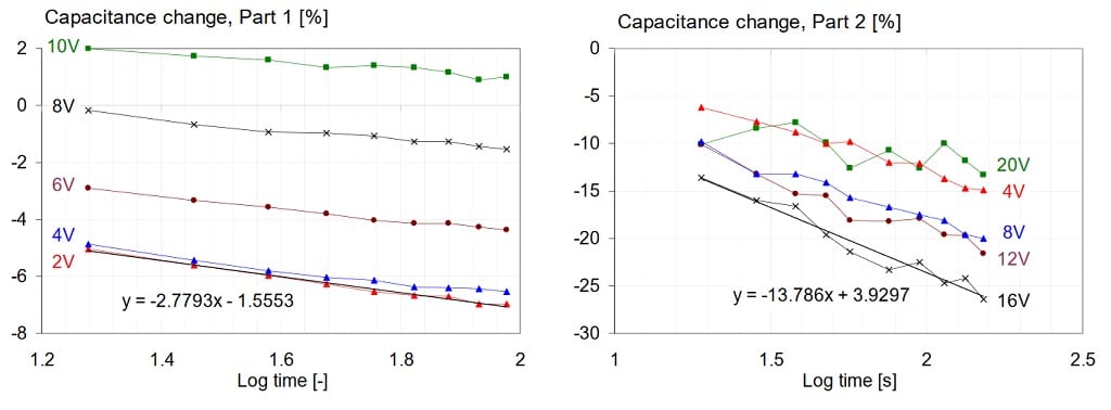
Figure 16: Comparison of capacitance change with time, on two different parts, after DC bias is applied. Left graphs: Part-1 from Vendor-A, 47uF 1206-size 6.3V X5R. Right graph: Part-2 from Vendor-D, 4.7uF 0805-size 16V X7R part. Note the logarithmic time scale on the bottom plots
Note that the relative relaxation after the first step in the capacitance value appears to be exponential. This is illustrated by the good fit of a straight line over the percentage capacitance change as a function of the logarithm of time. Note also that the strongest decay occurs at relatively moderate bias. The same effect is also shown on the 3D capacitance-bias-frequency plots, see Figures 17 and 18. The slow-relaxation part (Figure 18) exhibits a noticeable drop of capacitance even after 100 seconds of dwell time as the bias voltage steps to smaller absolute values (look at the left edge of plots).
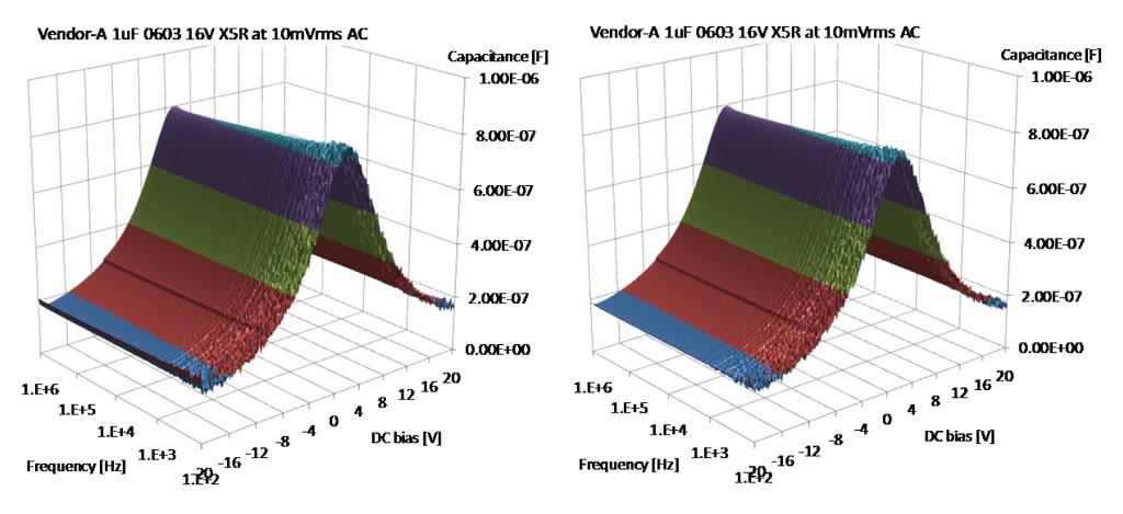
Figure 17: Capacitance surface plot as a function of frequency and DC bias on a quick relaxation part. Left plot: readings taken 10 seconds after changing bias. Right plot: readings taken 100 seconds after changing bias.
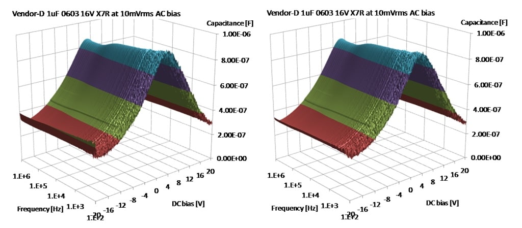
Figure 18: Capacitance surface plot as a function of frequency and DC bias on a slow relaxation part. Left plot: readings taken 10 seconds after changing bias. Right plot: readings taken 100 seconds after changing bias.
Temperature dependence
Class II ceramics have a standardized window of allowed temperature dependence for each sub-class. The two typical Class II categories, X5R and X7R, both have a maximum of +-15% allowed change of capacitance with temperature in the temperature range of -55 to +85 and -55 to +125 degC, respectively. The temperature dependence is specified with no DC bias. To see whether the temperature has any impact on the DC bias dependence, a few parts were tested at various temperatures.
The sample to be measured was soldered on the small test fixture (shown in Figure 3) and the setup was calibrated at room temperature. The fixture then was put in a temperature chamber and the calibration was rechecked at the various temperature settings to make sure that the same calibration for the fixture and the portion of cable inside the test chamber is valid over the entire temperature range used.
The DC bias dependence of the DUT was measured at a series of temperature settings from -5 degC to +70 degC. Since at each temperature point the DC bias dependence test takes about half a day, the number of temperature points was limited to the following sequence: -5 degC, +20 degC, +45 degC, +70 degC, -5 degC. The last temperature point was added to check for any long-term drift or memory. The DC bias dependence was measured with a frequency independent 10mVrms AC bias.
The 10mVrms AC bias is small enough that even if the AC level across the capacitor deviates from the calibrated level because of the change of capacitance, it has negligible effect on the DC bias sensitivity. The data shown here was collected on a 1uF 0603-size 16V X5R sample from Vendor B.

Figure 19: Variation of capacitance with temperature at 100 Hz. The maximum capacitance as a function of DC bias is recorded. Absolute capacitance values on the left, relative capacitance values on the right.
Figure 19 shows the maximum capacitance at 100 Hz. Note that the maximum capacitance occurs at a slight positive bias (see Figure 20), because the DC bias was sequentially stepped from -20V to +20V. The relative change of capacitance in the -5 … +70 degC temperature range is less than 10%. The temperature coefficient is positive.
The starting and finishing data points at the same -5 degC temperature are within 1% of value. Figure 20 shows the actual DC bias sensitivity curves at different temperature values. Absolute capacitance values are shown on the left, normalized relative change of capacitance curves are shown on the right. Note the tight tracking of normalized curves, indicating that the bias dependence does not depend on the temperature. 3D plots at -5 and 70 degC are shown in Figure 21.
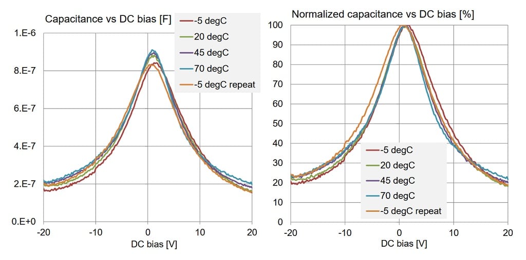
Figure 20: DC bias sensitivity curves of a 1uF 0603-size 16V X5R capacitor from Vendor B at different temperature values.
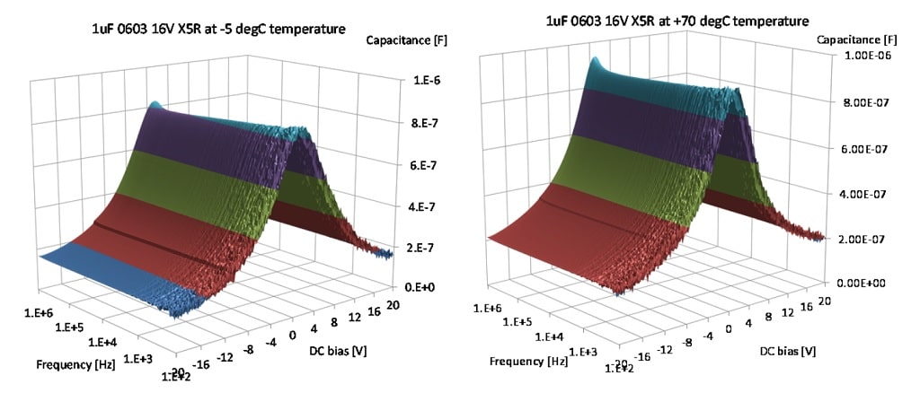
Figure 21: Capacitance versus DC bias and frequency at -5 degC temperature (on the left) and +70 degC temperature (on the right)
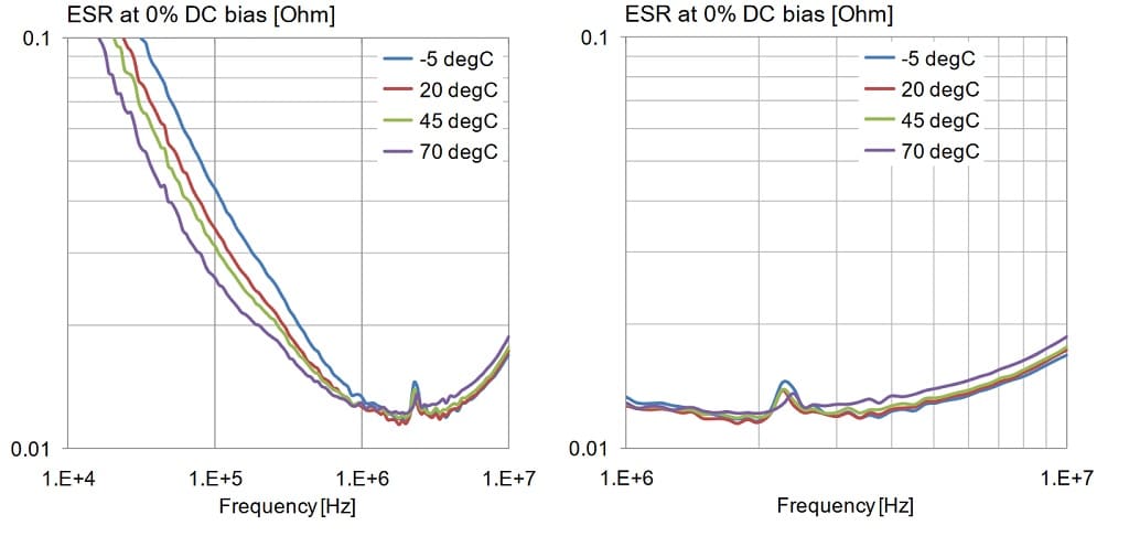
Figure 22: Variation of ESR with frequency, DC bias and temperature. Upper plots: temperature dependence with zero DC bias, full view on the left, zoomed view on the right. Lower plots: temperature dependence with 50% DC bias, full view on the left, zoomed view on the right.
Figure 13 showed that at room temperature ESR does not depend on DC bias above the series resonance frequency, but it changes together with the change of capacitance below the series resonance. Figure 22 shows a similar trend below the resonance; whether capacitance changes due to bias or temperature, ESR changes with it. Around and above the series resonance we can identify two trends: a) with increasing temperature ESR goes up and b) the piezoelectric resonance increases ESR more at elevated temperatures.
V. How all this may impact our designs
Ceramic capacitors are widely used in today’s electronic circuits. Many of them find applications in power distribution networks. In high-speed data links they are used as DC-blocking capacitors and occasionally as part of RC terminations. Analog circuits also use them for timing and DC blocking applications. In the next sections we will look at two power-distribution applications, where most of the high-density MLCCs are used.
Paralleled Capacitors
There are two different application categories in PDN, where the DC and AC bias dependence of MLCCs may need to be taken into account. The first application is, when we use MLCCs of different capacitance values in parallel (Figure 23). If the capacitors are assumed to be ideal, as shown on the left of the figure, all what we need to do is to sum up the different capacitances as they change with DC and AC bias. When their parasitics are also taken into account, the changes of the series and parallel resonances need to be considered as well. The change of capacitances will shift the series and parallel resonances to higher values and Q may also change slightly. If the relative rate of capacitance change is the same for all capacitors, what we get is mainly a shift of the impedance profile to higher frequencies and higher Q at the resonances.
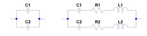
Figure 23: Equivalent schematic diagram of two parallel-connected capacitors. Left: without parasitics. Right: with parasitics.
The worst case occurs, when some of the paralleled capacitances decrease, while some others either don’t or actually might increase, perhaps due to the AC bias conditions.
Such a scenario is illustrated with measured data in Figure 24. Two capacitors were parallel connected in the test fixture: a 1uF 0603-size 16V X7R part from Vendor-D and a 47uF 1206-size 6.3V X5R part from Vendor-E. The minimum around 1 MHz is from the series resonance frequency of the 47uF part. The minimum around 7 MHz is the series resonance frequency of the 1uF part. The peak around 4 MHz is the anti-resonance between the capacitance of the 1uF part and inductance of the 47uF part. Note that all three resonances move towards higher frequencies, indicating that the capacitances of both parts decrease with increasing DC bias.

Figure 24: Impedance magnitude of two parallel-connected MLCCs of different kinds.
Capacitors in LC filters
Probably one of the worst situations is when multiple components joined in the same network, react to DC and AC biases in opposite directions. A typical scenario of this kind is when we use series inductors or ferrite beads for enhanced filtering, followed by shunt capacitors.

Figure 25: Equivalent schematics of a PI filter with series ferrite element and parallel MLCC at the output. Left: setup with no DC current bias through L1. Right: setup with DC current bias through L1.
If this filter circuit has to handle substantial DC current and the inductive element is not properly sized, its inductance may drop due to the DC current flowing through the part. If at the same time the filtered DC voltage reduces the capacitance of the MLCC part at the output of the filter, we end up with reduced inductance and reduced capacitance, resulting in a significant shift of the filter’s cutoff frequency. This effect was tested with the circuit shown in Figure 25.
The circuit under test was a simple PI filter, composed of two bypass capacitors and a series ferrite bead. The C1 capacitor on the input side of the filter was a 390uF 16V organic semiconductor type bulk capacitor. An organic semiconductor capacitor was chosen to mimic a low value of input feed impedance, and because they are known to have little or no DC and AC bias dependence. The C2 capacitor on the output was a 47uF 6.3V X5R 1206-size MLCC from Vendor-E. The L1 series element was a commercially available ferrite bead, rated for 2A maximum current.
The filter was measured with the Gain/phase test port of the E5061B LF-RF network analyzer by measuring the ratio of voltages at the output and input. Voltage transfer ratio was measured instead of transfer impedance (Z21) because in typical such applications the input feed comes from a higher-current rail, effectively imposing noise voltage across the input, as opposed to noise current, which would be the condition for transfer impedance [5]. The input impedance of both test ports was switched to 1 MOhm, which means we measure the unloaded output voltage of the filter.
Figure 26: Output/input voltage transfer function of the LC filter shown in Figure 21. Parameter: DC bias voltage.
Figure 26 shows the measured voltage transfer function with DC bias voltage applied across the capacitors, but no DC current through L1. The DC bias voltage was stepped from 0V to 10V (intentionally stressing C2 beyond its rated voltage) in 0.5V increments. The left graph of the figure shows the wide-band view of the transfer function from 100 Hz to 10 MHz.
As expected, at low frequencies we get no filtering. We notice some attenuation building up around 10 kHz. Before the transfer function gets to the steep slope, we get a minor peaking from the inductance of the ferrite and capacitance of C2. The steep slope eventually flattens out beyond 1 MHz. As a function of DC bias voltage, we see no change below 10 KHz and above 1 MHz. The peak frequency and the corresponding cutoff frequency of filtering slope, however, do move significantly.
With 0V bias the peak is at 24 kHz; with 10V bias the peak is shifted to 55 kHz. The graph on the right of Figure 26 shows the same data, zoomed between 10 kHz and 100 kHz. The following figures summarize the filter performance with a combined bias of DC voltage across the capacitors and DC current through the ferrite.
Figure 27: Transfer function of the filter shown on the right of Figure 19. The four plots show data with 0, 2, 4 and 8V DC bias voltages. On all four plots the parameter is the DC current through the ferrite.
Figure 28: Transfer function of the filter shown on the right of Figure 19. The four plots show data with 0, 0.5, 1 and 1.5A DC bias current through the ferrite bead. On all four plots the parameter is the DC bias voltage across the capacitors.
Figure 29: Transfer function of the filter shown on the right of Figure 19. The two plots show the cumulative transfer responses from Figures 21 and 22. Left plot: bias range limited to 0-4V and 0-1A. Right plot: bias range is 0-16V and 0-1.5A.
In Figure 29 we show all data traces from the previous plots. The plot on the left has the DC bias voltage and current limited to the reasonable ranges of 0-4V and 0-1A, respectively. The 4V and 1A DC bias limits are 63% and 50% of the rated 6.3V and 2A limits, respectively. There are two ranges marked on the plot along the two axes: the range of transfer-function magnitude variation at 260 kHz is 50 dB; the range of frequency variation at the -50 dB level is approximately 3.2 : 1. The plot on the right shows all traces for the full measured 0-16V bias voltage and 0-1.5A bias current ranges. There are two ranges marked on this plot, too: at 260 kHz the transfer-function magnitude variation is 68 dB; the range of frequency variation at the -50 dB level is approximately 7.2 : 1.
Conclusions
Over the past years, multi-layer ceramic capacitors have undergone significant improvements. The volumetric density has increased several folds. This unfortunately resulted in a big increase in DC and AC bias sensitivity for many parts. In particular, X5R and X7R parts, which previously showed only modest bias dependence, exhibit capacitance drops, which were previously seen mostly from Class III ceramics. The increased bias dependence creates additional challenges for users during the design and validation phase, and increases design complexity, since filters with otherwise identical filtering requirement now may require different component selection if they need to work in different bias environments. To help the users, all major vendors today supply at least DC bias information with their MLCC parts. Even so, an additional challenge for the user is how to fold the bias-dependent vendor data into the simulation environment.
Measured data collected during the study showed that the bias dependence for the same nominal part from different vendors can be very different. Moreover it was shown that bias sensitivity of X7R parts is not necessarily better than that of X5R parts, sometimes not even from the same vendor. It was also shown that in addition to an immediate change of capacitance with the applied bias, there is also a longer exponential relaxation, which can change capacitance further by as much as 25% over the course of a few minutes. It was found that the DC bias sensitivity of capacitance does not depend on the temperature. However, ESR does depend on the temperature at high frequencies, and it does depend on the temperature and DC bias around the piezoelectric resonance frequency.
Some vendors started to offer improved, low-sensitivity parts; one of those was shown in Figure 10 (standard X5R and improved X5R parts from Vendor-F). Vendors now also have the option to meet the requirements of the new JEITA standard [6], which sets a limit for the capacitance variation as a function of DC bias, and the AC test level is also reduced to better match the typical applications.
Acknowledgment
The authors wish to express their thanks to the vendors, who supplied samples for the study. Special thanks go the Mark D. Waugh from Murata, and John Prymak and Peter Blais from Kemet, for their valuable comments and discussions.
References
[1] Kemet capacitor catalog file F3102CE.pdf from www.kemet .com
[2] H. Fröhlich: Theory of Dielectrics – Dielectric Constant and Dielectric Loss. Oxford at the Clarendon Press, 1958.
[3] Mark D. Waugh, “Design solutions for DC bias in multilayer ceramic capacitors,” Ceramic Industry, October 2009. http://www.ceramicindustry.com/Articles/Advanced_Ceramics/BNP_GUID_9-5-2006_A_10000000000000668375
[4] Novak-Mori-Resso, “Accuracy Improvements of PDN Impedance Measurements in the Low to Middle Frequency Range,” Proceedings of DesignCon 2010, Santa Clara, CA, February 1-4, 2010
[5] Novak-Miller: Frequency-Domain Characterization of Power Distribution Networks. Artech House, Canton, MA, 2007.
[6] JEITA standard RCX-2326: Fixed capacitors for use in electronic equipment – Surface mount multilayer ceramic capacitors, Class 2A
Author(s) Biography
Istvan Novak is a Senior Principle Engineer at Oracle. Besides signal integrity design of high-speed serial and parallel buses, he is engaged in the design and characterization of power-distribution networks and packages for mid-range servers. He creates simulation models, and develops measurement techniques for power distribution. Istvan has twenty plus years of experience with high-speed digital, RF, and analog circuit and system design. He is a Fellow of IEEE for his contributions to signal-integrity and RF measurement and simulation methodologies.
Barry Williams is a principal engineer and a member of the technical staff at Oracle-Sun Microsystems since 2005. Before joining Oracle-Sun Microsystems, he worked for 17 years as principal engineer at Digital Equipment Corp – Hewlett Packard Co working in the VAX and Alpha Systems groups. Authored a book titled Power Distribution Systems for Electronic Circuits, and has co-authored several DesignCon papers that were presented. Graduate of Northeastern University.
Jason R. Miller is a Principle Hardware Engineer at Oracle Corporation where he works on ASIC development, ASIC packaging, interconnect modeling and characterization, and system simulation. He has published over 40 technical articles on the topics such as high-speed modeling and simulation and co-authored the book “Frequency-Domain Characterization of Power Distribution Networks” published by Artech House. He received his Ph.D. in electrical engineering from Columbia University.
Gustavo J. Blando is a Principle Hardware Engineer with over ten years of experience in the industry. Currently at Oracle Corporation, he is responsible for the development of new processes and methodologies in the areas of broadband measurement, high speed modeling and system simulations. He received his M.S. from Northeastern University.
Nathaniel Shannon is a Signal Integrity Hardware Engineer at Oracle Corporation. He is responsible for the development of signal integrity modeling and simulations of high speed serial and parallel buses as well as simulations of power distribution networks. He received his M.S. from Northeastern University.

