

This article by Knowles Precision Devices introduces basic facts of microstrip filters, how it works and what is their performance.
Microstrip filter technology was first released in 1952, since then, numerous advancements in both dielectric material manufacturing and thin film processing techniques have led to the adoption of microstrip filtering for a wider range of applications, especially at mmWave frequencies.
An Overview of How Microstrip Technology Works
At a high level, microstrip refers to a type of planar transmission line technology that consists of a conducting strip separated from a ground plane by a dielectric substrate as shown in Figure 1.
More specifically, the design and construction of a microstrip filter is similar to the way circuits are configured on a printed circuit board (PCB).
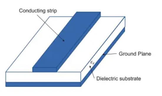
However, a key distinction of a microstrip filter is that the metal conductor patterns printed on the solid dielectric substrate are there to create resonators rather than just interconnects. The metal circuit patterns of strip elements are placed on a solid dielectric insulating layer with a metal ground layer below the dielectric.
The fields surrounding the strip permeate two different media, with part of the field in the substrate and another in the air above the strip. The higher permittivity of the dielectric substrate causes the electric field to concentrate in the substrate, which means field losses due to material choice become a factor. Standard PCB materials like FR4 can be used below 1GHz for low Q filters. Lower loss and increased Q can be achieved using ceramic materials.
This type of printed transmission line is a popular filtering option since these filters can cover a broad frequency range, are economical to produce, and are often lighter and more compact than alternative transmission line technologies such as waveguide.
Overcoming Issues with Loss for Microstrip Filters
The biggest concern with microstrip filters is the loss experienced compared with other transmission-line and waveguide filtering approaches. However, the evolution of high-k materials, such as our PG, CF, and CG ceramics, is making it possible for RF engineers to develop low-loss microstrip transmission-line filters.
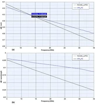
In Figure 2, we show how a microstrip transmission-line configuration using our PG ceramic reduces loss compared to a microstrip filter using a common RO4350 LoPro dielectric. In this comparison, we used the same material thickness, metal conductivity, and 50-Ω microstrip transmission line in both configurations.
Beyond loss reduction, when a filter manufacturer also engineers the substrate material, this offers another key benefit – the ability to substantially shrink the wavelength of the electromagnetic waves propagating along a microstrip transmission line. For a microstrip line, wavelength is determined using the following equation:
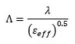
Λ = Wavelength in microstrip
λ = The free-space wavelength
εeff = The effective dielectric constant, which depends on the dielectric constant of the substrate material and the physical dimensions of the microstrip line.
Let’s look at Knowles Precision Devices catalogue surface mount bandpass filter the B099NC4S, which is a popular X band filter, as an example. This filter has dimensions of 10.2mm x 3.8mm, or in terms of free space wavelength at 12GHz, 0.4λ x 0.15λ. We can use the material advantages we achieve by developing our own substrates to shrink the wavelength inside the filter (per the equation above) so that the filter ends up quite small compared to any radiation outside the filter – i.e. in free space.
This also means we can develop small-scale microstrip surface mount technology that is ideal for mmWave applications. And since we can make the physical size of antennas at mmWave frequencies sufficiently small, it makes sense to build complex antenna arrays on chips or the PCB directly using a microstrip approach. Therefore, entire devices including antennas, couplers, filters, and power dividers can be formed by creating metallized patterns on the substrate.
The Capabilities of Microstrip Filters
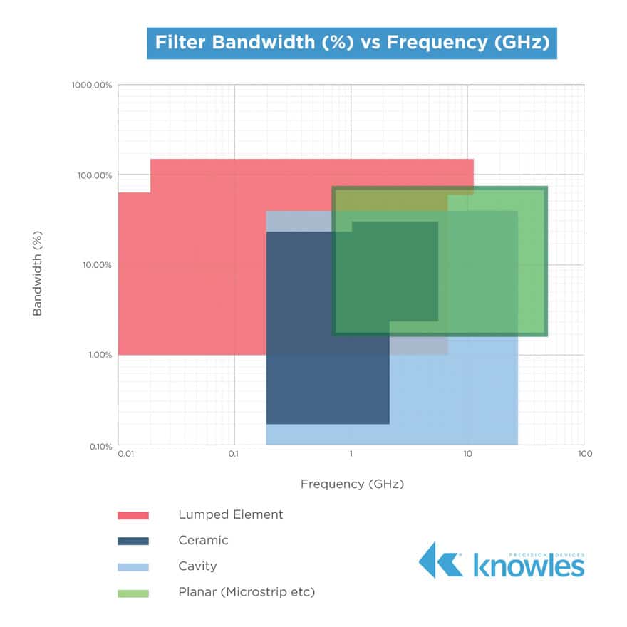
Variety of bandpass, lowpass, and highpass filters from 1GHz to 42GHz (and beyond) can be made using thin-film microstrip technology. Knowles Precision Devices capabilities are shown in green field at Figure 3.
Microstrip filters offer the following key benefits:
- Temperature stability from -55°C to 125°C
- A reduction in filter size versus using a typical PWB of up to 20x using our CG material, 10x using CF, or 3x using PG
- High repeatability since thin film manufacturing provides precise manufacturing performance with no tuning required
- custom microstrip filters for higher frequency ranges can be developed

