
This article explains the basic key parameter of capacitors – capacitance, capacitive reactance and its calculation. The article also includes capacitance calculations of series / parallel connection and E tolerance fields standards.
Key Takeaways
- This article explains the basic concepts of capacitance, including its definition and calculation methods.
- Capacitance reflects a capacitor’s ability to store electric charge, influenced by factors like dielectric material and electrode distance.
- The article discusses capacitive reactance, outlining its dependence on frequency and providing related formulas.
- Capacitance calculations could involve series and parallel connections, affecting overall capacitance values accordingly.
- It also addresses standardized capacitance values and tolerance ranges based on international standards EIA/IEC 62.
Capacitance Definition
The Capacitance is determined by, among other things, the characteristics of the dielectric material. International standards speak of the Dielectric Constant or permittivity, designated by the symbol ε.
Description
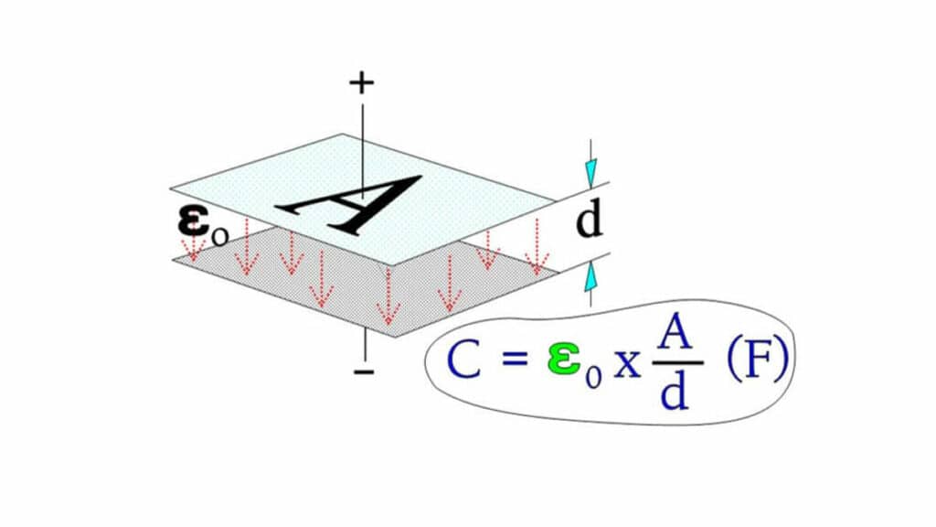
A capacitor serves as a reservoir for electric charges. The size of the ”reservoir” is called capacitance and is expressed in the quantity F(arad) or As/V. The principle Figure 1. shows how the capacitance is directly proportional to the active area A and to the dielectric constant and inversely proportional to the distance between the electrodes. The formula in the figure is applicable to vacuum and air.
A = area (m2),
d = distance between electrodes (m),
ε0 = dielectric constant for vacuum (≈air) = 1×10⁻⁹/36π.
If the electric charge quantity of the capacitor is designated with Q (As), then the general formula 1 is valid.
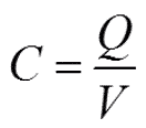
……………………………… [1]
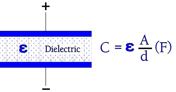
If we now insert an insulator material between the electrodes as shown in Figure 2., the formula in the figures 1. and 2. get the following general expression:

………………………………. [2]
εr is a relative number – the relative dielectric constant – which tells us how many times the capacitance is magnified when we exchange the air gap between the electrodes with different dielectric materials. That’s the relative dielectric constant εr which is given in technical tables and catalogues.
Table below shows dielectric constant of the most common materials.

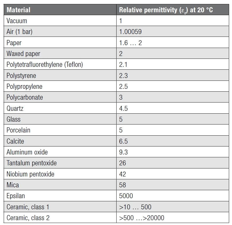
Some more organic dielectric material constants can be found in article here.
Capacitive Reactance
If we change polarity in Figure 2. by applying an AC voltage over the capacitor, it will cause a certain resistance in the circuit, a so called capacitive reactance, XC, expressed in ohms.
The reactance is inversely proportional to frequency according to the formula

…………………….. [3]
- ω = 2 x π x f,
- f = frequency in Hz,
- C = capacitance in F.
Measure of miniaturization
The desired miniaturization of different capacitor types can be expressed in different ways. The smallest rated voltage for electrostatic capacitors often is more than enough for the application. Hence we usually disregard the voltage and compare the various types by means of their maximum possible C/V rate which means capacitance C per unit volume V (d * A in the Figure 1). According to the Formula [2] we get C/V = ε0 * εr * A/(d * A * d) = ε0 * εr /d2. The rate C/V will be at maximum for dmin, i.e., for VRmin.
In electrolytic capacitors the rated voltage plays a greater role because it can be adopted also to very low working voltages. Here the capacitors are grouped according to their charge quantity, that is to CR*VR. We refer to the CV product.
Capacitance Calculation and Connections
If we connect capacitors in parallel as shown in Figure 3. the active area (and hence the capacitance) increases with all additional capacitor elements.

Formula for the total capacitance of connections in parallel:
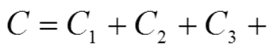
……………. [4]
Figure 4. shows in principle how connection in series increases the dielectric thickness without changing the charge quantity. The capacitance decreases proportionally to the increase of dielectric thickness.
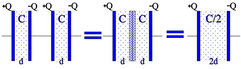
The figure shows a simplified picture of series connection with two equally large part capacitors. If we instead choose capacitor elements of unequal size the charge quantities on the different electrodes still will be equally large, i.e. Q = CV = C1V1 = C2V2 = C3V3; Q/C = V; Q/C1 = V1; Q/C2 = V2; Q/C3 = V3…But V1 + V2 + V3 +….= V. This gives us in general the total capacitance for Series connection:
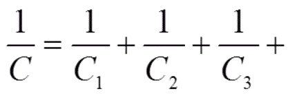
………….[5]
Mixed dielectrics
So called mixed dielectrics have become more and more common. They consist of different film materials in the same capacitor. For example by winding a capacitor with both a paper and a polyester film dielectric we combine the excellent self healing properties of paper and the relatively high insulation resistance of polyester. In principle it’s still a question of two capacitor elements in series connection, with the same area and the dielectric thickness d1 + d2. Then the relation we depicted above is valid: Q = VC = V1C1 = V2C2; V1 x ε1 x A/d1 = V2 x ε2 x A/d2; if we denounce the electric field intensity E we then obtain ε1 x E1 = ε2 x E2, or in general
ε1 x E1 = ε2 x E2 = ε3 x E3 =
……………………… [6]
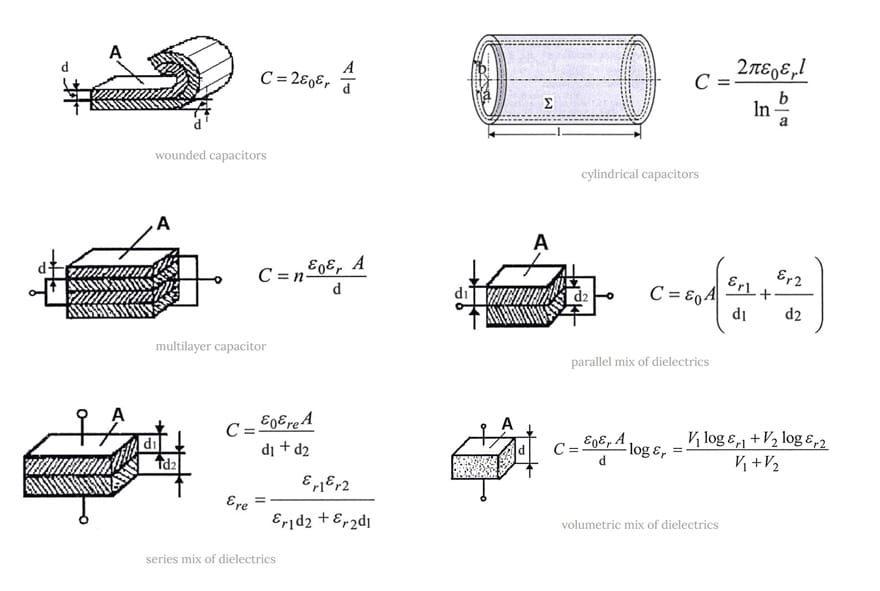
Other non-plate and various geometry capacitance calculations
The capacitance calculation by equation [2] and illustrated in figure 2. are based on plane capacitor type. However, there are many other capacitor construction types and geometries on the market. See the theoretical capacitance value calculation for some of other geometries as well as mixed dielectric situations below:

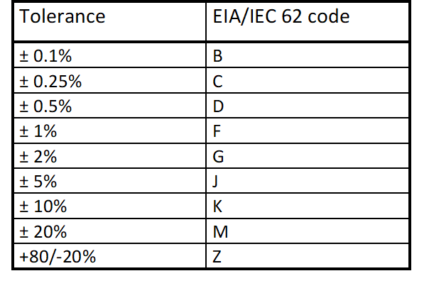
Capacitance standardized values and tolerance
Following international standards EIA/IEC 62, capacitance values and tolerances are standardized as follows:

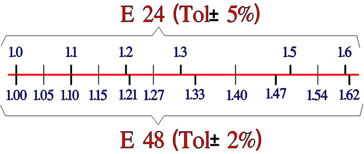
E range
Capacitance is following standardized “E ranges” defined per logarithmic-steps such as E3, E6 … E24, E48 steps.
Naturally, the selected E-range is also linked to the tolerance field – not to overlap between the next capacitance tolerance range – see bellow.

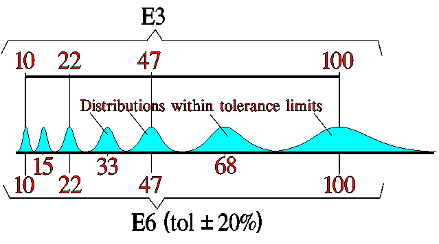

Specific capacitor technologies’ E range is driven by its capability to produce reproducible and tight tolerance capacitance value in mass production. You can find the relevant capacitance values and tolerance ranges defined in manufacturers’ catalogues.
Frequently Asked Questions about Capacitance and Dielectrics
Capacitance is the ability of a capacitor to store electric charge. It depends on the electrode surface area, the distance between plates, and the dielectric constant of the insulating material. It is measured in farads (F).
The dielectric constant (εr) indicates how much the capacitance increases when air is replaced by another insulating material. Higher dielectric constants result in higher capacitance values.
Capacitive reactance (Xc) is the opposition a capacitor presents to alternating current. It is inversely proportional to both frequency and capacitance, meaning higher frequency or larger capacitance lowers reactance.
In parallel, capacitance values add up, increasing total capacitance. In series, the effective capacitance decreases, as the dielectric thickness effectively increases.
International standards (EIA/IEC 62) define capacitance values in E‑ranges (E3, E6, E24, E48, etc.) with specific tolerance fields to ensure consistency across manufacturers.
How to Calculate and Understand Capacitance
- Identify capacitor structure
Determine the plate area (A), distance between electrodes (d), and dielectric material used.
- Apply the capacitance formula
For a plate capacitor use the formula C = ε0 × εr × A / d, where ε0 is the permittivity of free space and εr is the relative dielectric constant. For wound and other structures use formula noted in this article.
- Consider AC behavior
For alternating current, calculate capacitive reactance with Xc = 1 / (2πfC), where f is frequency in hertz.
- Evaluate connections
For parallel connections, add capacitances directly. For series connections, use the reciprocal formula: 1/Ctotal = 1/C1 + 1/C2 + …
- Check standardized values
Compare your calculated capacitance with standardized E‑ranges (E6, E24, E48) to select the closest available component.

