
Source: EDN article
Istvan Novak, PhD, Senior Principle Engineer at Oracle is in his three EDN articles [4], [5], [9] introducing some tips and tricks for own component measurementand PCB fixture preparation.
Bypass capacitors are used in large numbers in power distribution networks. Most vendors today supply not only typical characteristics, but also various simulation models. Nevertheless, doing our own characterization of these components is still useful and often necessary. In the first chapter, I’ll show you how to create simple home-made solder-wick fixtures for these measurements. Fixed-geometry fixtures with defined return paths for more consistent measurements are introduced in the second PCB Fixtures chapter.
For bypass capacitors, measuring impedance over a reasonably wide frequency range is the way to go. This gives us the small-signal equivalent behavior of the part. By post-processing the complex impedance, we can obtain the capacitance, effective series inductance (ESL), and effective series resistance (ESR) as functions of frequency. If needed, DC- and AC-bias-voltage dependence and temperature may be added to the mix of input parameters. All these have been described in earlier publications [1]. Similarly, the instrumentation and measurement setup for this purpose is well established [2]. To measure the impedance of bypass capacitors with high capacitance and low ESR, a good choice is a suitable vector network analyzer [3] in the two-port shunt-through connection.
Once we have our instrumentation ready, the next challenge is to decide how we connect our sample to the instrument. For quick and simple measurements, home-made fixtures work just fine.
Solder-wick fixture
This is a simple and rudimentary fixture, yet it works amazingly well at low frequencies. We start with two thin and flexible coaxial cables, with connectors at one end and pigtails at the other. You could use an RG-178 SMA jumper and cut it in the middle. This gives us two cables of identical length. The type of connector does not matter much at low frequencies; SMA connectors are relatively small, low cost, and readily available. After cutting, the cables should be long enough to bridge the distance between the network analyzer and our fixture, placed on the bench in front of it (if we have a choice, we should always opt for the shortest cable that can make the connection).
Strip the plastic jacket at the open ends, untangle the braids for about ¼”, and create pigtail connections. Next, cut two pieces of 1” solder wick, slide on short heat-shrink tubes, solder the two coax cables in a series fashion, slide the heat-shrink tubes in place, and finally activate the heat-shrink tubes with a heat gun. We get a flexible fixture shown on the top of Figure 1. We need to mark the strips; which is the one connecting the center wires, and which is connecting the braids of the coax cables. We can use colored heat-shrink tubes, or, as in Figure 1, the somewhat longer heat-shrink tubes mark the return (braid side) of the coax.


Figure 1 Solder-wick fixture (top) and a D-size capacitor in the fixture (bottom).

The capacitor can be placed between the two exposed solder-wick conductors; this will create a two-port shunt-through measurement scheme. On the bottom of Figure 1, a D-size (7.3 × 4.3 mm) capacitor is shown in the fixture. This fixture is best suited for pressure-mount connections, not for soldering. The benefit is that by using pressure contacts, we avoid heat stress to the component and can swap out samples quickly. The pressure-mount connection can be implemented by a spring-loaded plastic or wood clip, or we can just squeeze the fixture between our fingers with the component in place. If we are worried about the error caused by our body impedance, we can grab the solder-wick electrodes with our fingers but without a capacitor in place and take the impedance reading. As long as it is much higher than the impedance of the capacitor, we can ignore this error.
If we use short cables and limit the frequency to below 10 MHz, a simple response-through calibration on the VNA is enough. Note that the calibration and measurements are done without changing/disconnecting the cables, which improves the consistency of the measurements.
We should also make additional reference measurements. We have to measure the fixture with no DUT in place (open) and with a short, similar in size to the DUT we want to measure later. Figure 2 shows the impedance readings for these reference cases. The photo of our shorting device is shown in Figure 3. An extra capacitor sample was taken and the terminals on the bottom of the part were shorted with a strip of solder wick.

Figure 2 Impedance magnitude of Open and Short

Note that the impedance of the short reference piece is not exactly zero; it has finite resistance and inductance. For measuring really low impedances, we would need to characterize our shorting device, and do a more complex calibration.

Figure 3 D-size Short reference

In this very rudimentary fixture there is direct connection between the two VNA ports through the braid, which creates a “sneaky path”. As a result, what we get for the short reading (and for all other readings) is a mix of, a) the actual impedance of the DUT, b) some contact resistance, and c) the residual error created by the sneaky path. The open and short readings give us an impedance range where we can trust our data with this fixture with just a response-through calibration: the DUT impedance should be at least 3-5× (preferably 10× or more) away from these limits. The traces corresponding to open and short run around 20 kΩ and 2 mΩ at low frequencies, respectively. The rising tail of the short impedance trace is due to its inductance. Note also that the lower measurement limit set by the instrument noise was below 0.1 mΩ.
Figure 4 shows the impedance magnitude of ten DUTs measured with this fixture. The data was collected by pressing the solder wick against the capacitor terminals by hand.

Figure 4 Impedance magnitudes of ten capacitor samples

Readings are close at 1 kHz indicating close tolerances on the measured 470 µF capacitors. The lines begin to deviate beyond 10 kHz and hit maximum spread around the series-resonance frequency of 1 MHz. Considering that for bulk capacitors the data sheet guarantees only a maximum value of ESR (but no typical or minimum), the spread we see here is considered to be typical.
Of course, with this simple fixture, we also need to consider the spread and consistency of contact resistance. Above the series-resonance frequency, the spread continues. The upslope between one and ten megahertz represents inductance. Inductance is related to current-path geometry. As the body size and shape of these capacitors is very consistent, the likely source of inductance spread is the variation of the loop size of the solder-wick connections as we press the fixture to the DUT.
We can always re-measure the outlier samples. This will tell us whether the data needs to be updated or in fact some parts were outliers. We need to remember to periodically clean the surface of the solder-wick strips to remove contamination and we also have to make sure that the component terminals are clean.
In summary, this simple fixture may have some downsides: the sneaky path raises the error floor, the flexible solder-wick connections make the discontinuity between the cables more uncertain, and the contact resistance can vary. But, for measurements below 10 MHz and above a few milliohms in values, the simple construction, ease of connection, and simplicity of calibration far outweigh the drawbacks.
PCB Fixtures to improve component measurements
The fixtures discussed in previous chapter have limitations because the shape of the current path isn’t controlled. In the solder-wick fixture, the shape of the flexible connections will vary depending on how you achieve the pressure-mount connection. To get more consistent results, use fixed-geometry fixtures with defined return paths. You have two options: a) generic fixtures, which can take a large variety of different DUT body shapes and sizes in the same fixture, and b) fixtures with dedicated footprints for specific DUTs. Here, I show you generic fixtures [6].
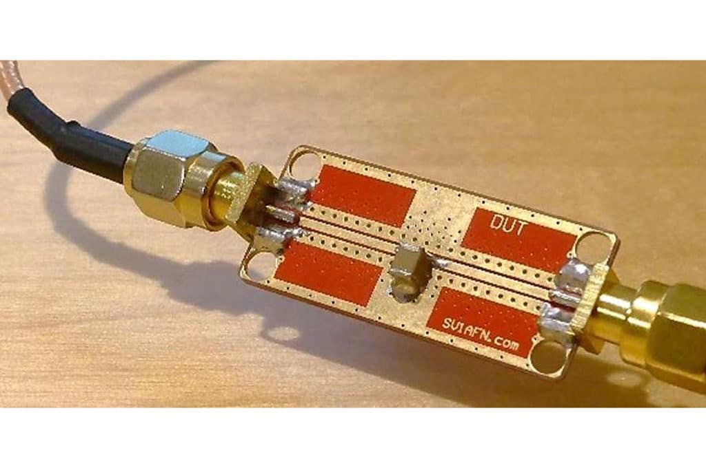
You can create generic PCB fixtures from small co-planar 50-Ω traces that have exposed trace and ground next to each other on the same side of the fixture. The DUT can be connected between the trace and the ground shape, letting you use the Two-Port Shunt-Through measurement topology.
Having a sufficiently large ground shape next to the trace, you can accommodate many different case styles and sizes. Having connectors at the ends of the through trace provides quick connections, though you could also use permanently attached (soldered) cables. Soldered cables eliminate the need for separate cables with connectors at both ends, but makes the calibration a little bit more difficult. Figure 5 shows the unassembled panel of fixture boards. One panel provides eight identical fixture boards (though they carry different labels) that you can break away.

Figure 5. This Unassembled panel of eight fixtures contains three for calibration and five for component measurements. Source: SV1AFN
Three of the boards are labeled for calibration (OPEN, SHORT, LOAD) and five are labeled for measuring components (DUT). These fixtures also let you do a more comprehensive OPEN, SHORT, LOAD calibration, which I’ll explain and describe in later articles.
The panels are available with SMA male-female connectors attached, or with the loose male-female connectors shipped in the same package for you to solder them on. Figure 6 shows a female connector at one end and a male connector at the other end, which creates what is called an insertable piece—you can take a closed male-female connection, open it and insert the piece without the need of any adaptor.

Alternately, you can get the fixtures unassembled and solder SMA female connectors to both ends, which will conveniently take cables with male connectors on both cable ends.
The lines of the fixture are coplanar waveguide (CPW) over ground. The printed circuit material is FR4 and the board thickness is 0.8 mm. The gold-plated nickel over copper is 35 µm (1 oz.) and the line width is 1 mm with 0.254 mm separation to ground.
These fixtures can take any component size from 0402 (1 mm long) to D-size (7.3 mm long). The DUT sample in Figure 7 is a 1210-size ceramic capacitor.

With these fixtures, you also have the option of connecting the DUT in different ways. Mechanically and electrically, you get the most robust and most reliable connection if you solder the part to the fixture. If you want to reuse the fixture and want to speed the swapping of components, you can opt to use simple pressure mount, like we did with the solder-wick fixture, and you can reduce the contact resistance and improve consistency of your collected data by applying a dot of silver paste each to the component terminals. If you solder the component, push down the parts on the pads during soldering to improve measurement repeatability.
Using a VNA (Figure 8), you can characterize the component with a frequency sweep. If you want to start the sweep anywhere below a few times ten kilohertz and measure components that have low impedance at low frequencies such as low-ESR high-capacitance components, you run up against the cable-braid loop error. Depending on how you reduce the cable-braid loop error, the chosen solution may come with its own limitation at low or at high frequencies. For this article, I used a home-made common-mode choke, with an upper bandwidth of approximately 50 MHz. The data was collected in the 300 Hz to 30 MHz frequency range with simple THRU calibration.

Figure 8. Measurement setup shows the test board connected to a network analyzer through home-made common-mode toroid (black box). E5061B network analyzer courtesy of Keysight Technologies.
With soldered connections and a rigid fixture geometry, you can use this setup reliably up to higher frequencies as well. That is, if you’re willing to do more complex calibration. The tradeoff is between the start and stop frequencies of the sweep and the nature of components you want to measure.
Figure 9 shows the measurement result from the setup and DUT shown in Figs. 7 and 8. You make use of the Impedance Analysis Option [8] and the screen is set up for four simultaneous traces: Impedance magnitude (upper left), Effective Series Resistance, RS (upper right), Equivalent Series Capacitance, CS (lower left) and Equivalent Series Inductance, LS (lower right). The logarithmic horizontal scale starts at 300 Hz and ends at 30 MHz. The 70 Hz IF bandwidth (IFBW) setting provides a good compromise between fast sweep and low noise floor.

Figure 9. Measurement data of the 47 µF 1210 size ceramic multi-layer capacitor taken in the co-planar fixture.
The measurement result shows several familiar details. From 300 Hz to almost 1 MHz, the impedance magnitude slopes downwards, indicating capacitive impedance. The trace bottoms out at 850 kHz with a 2 mΩ value at the series resonance frequency. Beyond 850 kHz, the impedance magnitude slopes upwards, indicating the inductive region. There are smaller secondary resonances and inflection points between 1.5 MHz and 3 MHz, beyond which the impedance stays clearly inductive.
The effective series resistance plot (which is simply the real part of the measured complex impedance) on the upper right follows a similar pattern. At low frequencies it runs parallel to the impedance magnitude curve and their ratio is the dielectric loss tangent. You can read more about this in [4]. After a broad minimum near the series resonance frequency, the effective resistance also trends upward with a few secondary resonances. The lower left and right plots show the capacitance and inductance extracted from the imaginary part of the measured complex impedance. If you want to do the calculations yourself, you can use the following formulas. First, you convert the complex S21 values to complex impedance:

In the next step, take the imaginary part of the impedance and assume that it comes from capacitance or inductance. If the imaginary part of impedance comes from capacitance or inductance, you can use the following formulas, respectively:

Where ω is the radian frequency, or 2πf. You can apply both formulas simultaneously over the entire frequency and rearrange them for C and L. They will give the correct (positive) capacitance and inductance values in their respective portion of the frequency range.
Using these formulas with the data shown in Fig. 9, you get positive capacitance and negative inductance (that we just ignore) below 850 kHz. Above 850 kHz, you get positive inductance and negative capacitance (which, again, you just ignore). Finally, if you look at the extracted capacitance and inductance curves, you’ll see both are sloping downwards slightly. The capacitance curve slopes downwards due to the dielectric losses: the higher the loss tangent, the more pronounced slope you see. The inductance curve slopes down because of the finite size and thickness of the DUT. At low frequencies, the current path is determined by resistive losses and as a result the current spreads out utilizing a bigger part of the structure. At high frequencies, the current path is dictated by the path inductance, which is smaller in smaller loops. If the current has the opportunity to rearrange itself as frequency changes, it will flow in smaller loops as frequency goes up.
These co-planar fixtures are very universal, but they also carry some limitation. Similar to the solder-wick fixture, the co-planar trace represents not only a convenient way to attach a DUT, it also creates a “sneaky path” between the two VNA ports. Second, being generic, chances are that these fixtures will not match the geometry of the final use in your design. This latter, however, has an impact only on the inductance; the capacitance and ESR still can be assessed with high confidence. If you need a fixture that will correctly represent the mounted inductance of the part in our design, we need dedicated fixtures for each case size, matching the stackup, via structure, footprint and all horizontal connections between the capacitor and the power planes.
—Istvan Novak is Senior Principal Engineer at Oracle, with over thirty years of experience in high speed digital, RF, and analog circuit and system design. He is a Fellow of the IEEE, author of two books on power integrity, teaches signal and power integrity courses, and maintains an SI/PI website.
References
[1] “DC and AC Bias Dependence of Capacitors Including Temperature Dependence,” DesignCon East 2011, Boston, MA, September 27, 2011
[2] “Accuracy Improvements of PDN Impedance Measurements in the Low to Middle Frequency Range,” DesignCon2010, Santa Clara, CA, February 1-4, 2010
[3] Keysight E5061B ENA Vector Network Analyzer
[4] Solder-wick trick characterizes bypass caps, EDN, May 9, 2018.
[5] Make simple fixtures from SMA connectors, EDN, August 27, 2018.
[6] RF Experimenter’s PCB Panel of 8 pcs https://www.sv1afn.com/rf-experimenter-s-pcb-panel.html
[7] How to read the ESR curve http://www.electrical-integrity.com/Quietpower_files/QuietPower-22.pdf
[8] Impedance Analysis for the E5061B ENA LF-RF Vector Network Analyzer, Keysight Technologies. https://www.keysight.com/en/pd-1944859/lf-rf-network-analyzer-option-005-impedance-analysis-option
[9] PCB Fixtures improve component measurements, EDN, October 30, 2018

