

Samsung Electro‑Mechanics has introduced a dedicated silicon capacitor lineup targeting high‑performance semiconductor packages, AI servers, advanced automotive and aerospace electronics.
These Samsung Electro‑Mechanics ultra‑thin silicon capacitors combine semiconductor processing with capacitor functionality to deliver very low ESL, high capacitance density and stability up to 250 °C, making them attractive as high‑speed decoupling elements directly in or on the package.
Key features and benefits
- Ultra‑thin form factor for in‑package and embedded use
Silicon processing allows etched three‑dimensional structures in the silicon substrate, achieving several hundred nanofarads up to tens of microfarads in thicknesses down to around 60–70 µm for small parts and around 0.7–0.75 mm for larger multi‑rail devices. This profile is suitable for mounting inside advanced packages or embedding in organic substrates where z‑height is strictly limited. - Very low parasitic inductance for high‑speed decoupling
The lineup is optimized for low equivalent series inductance (ESL), with values in the under‑1 pH class according to the manufacturer. In practice, such low inductance helps to maintain power integrity for AI and high‑speed digital SoCs by reducing supply bounce and allowing clean, fast current transients at the die power rails. - High reliability and thermal stability up to 250 °C and above
The dielectric system and silicon technology are designed for stable capacitance over a wide temperature range, including harsh conditions such as AI servers with high junction temperatures, automotive under‑hood modules and aerospace electronics. Minimal capacitance drift with temperature simplifies derating and worst‑case analysis in mission‑critical designs. - Package‑style variants for different integration approaches
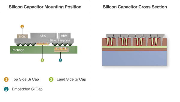
The tabled lineup includes LSC (land‑side capacitors for package mounting), DSC (device‑side capacitor modules with many power rails), and embedded types intended to be built into an organic substrate. This gives package designers options for both discrete assembly and true embedded decoupling. - Support for multi‑rail power architectures
Several part numbers support multiple power rails in a single silicon capacitor die (from 2 up to almost 200 rails), enabling localized decoupling of many power domains in AI accelerators, high‑core‑count CPUs or complex SoCs without populating dozens of discrete MLCCs per rail.
Typical applications
Samsung Electro‑Mechanics positions the silicon capacitor lineup for designs where ultra‑thin form factor, low ESL and high reliability are critical:
- AI and cloud server chipsets
Decoupling of high‑current core, memory and I/O rails directly at the package or interposer for GPUs, NPUs and custom AI accelerators in server and data‑center platforms. - High‑end networking and optical communication
Power integrity solutions for high‑speed SerDes, coherent optics and switch ASICs where low inductance and controlled impedance are key for jitter and signal integrity. - Automotive and aerospace systems
Power supply decoupling in autonomous driving ECUs, radar and lidar modules, and avionics where operating temperatures and reliability requirements exceed the capability of standard MLCC‑based solutions. - Mobile and wearable devices
Ultra‑thin smartphones, AR glasses and next‑generation wearables where z‑height is tightly constrained and integrating decoupling into the package or substrate helps free PCB area. - Embedded and system‑in‑package (SiP) modules
RF front‑ends, compact sensor modules and custom SiPs that benefit from integrating silicon capacitors into the substrate to shrink footprint and improve EMC.
Technical highlights
Samsung’s product news lists nine silicon capacitor variants, covering samples and mass production parts optimized mainly for DC decoupling in high‑speed digital and power‑intensive environments. The main electrical parameters are summarized below according to the manufacturer’s table.
Small LSC silicon capacitors (package‑mount)
| Part number | Status | Capacitance (nF) | LW (mm) | Thickness (µm) | Rails | Rated voltage | Breakdown voltage | Package |
|---|---|---|---|---|---|---|---|---|
| SCBCAP305L95EGNNWT | Sample | 3000 | 1.26 × 1.03 | 68 | 4 | 1.2 V | 3.7 V | LSC |
| SCBCAP105L95AGNNNT | Sample | 1000 | 1.26 × 1.03 | 68 | 4 | 1.35 V | 4 V | LSC |
| SCBCAP514L95AGNNNT | MP | 512 | 1.26 × 1.03 | 70 | 4 | 1.35 V | 4 V | LSC |
| SCBC5P254L95AGNNNT | MP | 256 | 1.26 × 0.51 | 70 | 2 | 1.35 V | 4 V | LSC |
| SCG98P105M86AGNNWT | MP | 1050 | 0.96 × 0.88 | 60 | 2 | 1.35 V | 4 V | LSC |
These devices are intended for land‑side mounting close to the package on the organic substrate. The combination of sub‑millimetre dimensions, around 60–70 µm thickness and up to 3 µF capacitance allows engineers to place effective high‑frequency decoupling as close as possible to the die bump field, complementing bulk decoupling on the PCB.
High‑rail‑count DSC module
| Part number | Status | Capacitance (nF) | LW (mm) | Thickness (µm) | Rails | Rated voltage | Breakdown voltage | Package |
|---|---|---|---|---|---|---|---|---|
| SCHVSP107MH1AGB9WT | MP | 103950 | 11.01 × 8.35 | 750 | 198 | 1.35 V | 4 V | DSC |
This DSC device effectively integrates a large total capacitance of about 104 µF distributed over up to 198 power rails. Such a module is suitable for advanced AI or networking packages where many individual rails require localized decoupling and common PCB real estate is limited. The larger body and thickness reflect its role as a package‑level power integrity component rather than a single‑chip discrete on a PCB.
Embedded silicon capacitors
| Part number | Status | Capacitance (nF) | LW (mm) | Thickness (µm) | Rails | Rated voltage | Breakdown voltage | Package |
|---|---|---|---|---|---|---|---|---|
| SCRLLC885MG5EGNNWT | Sample | 8800 | 2.00 × 2.00 | 738 | 2 | 1.2 V | 4 V | Embedded |
| SCRNKC166MG5EGNNWT | Sample | 17600 | 4.06 × 2.00 | 738 | 4 | 1.2 V | 4 V | Embedded |
| SCRNNC326MG5EGNNWT | Sample | 35000 | 4.02 × 4.02 | 738 | 4 | 1.2 V | 4 V | Embedded |
These embedded devices are designed to be integrated into the build‑up layers of an organic substrate, directly under or near the die. This approach further minimizes loop inductance and frees surface area for routing and components, which is important in very dense SiP or module designs.
All listed capacitors are specified for rated voltages in the 1.2–1.35 V range with breakdown voltages around 3.7–4 V, reflecting their intended use as high‑density decoupling elements for low‑voltage core and I/O rails in modern digital ICs. For exact electrical characteristics over temperature and frequency, designers should consult the respective manufacturer datasheets.
Design‑in notes for engineers
- Consider silicon capacitors as part of a power‑integrity stack‑up
These devices are best used together with conventional MLCCs and bulk capacitors. Use silicon capacitors for the very high‑frequency decoupling path close to the die, while larger MLCC arrays and polymer/bulk capacitors handle mid‑ and low‑frequency energy storage. - Exploit low ESL by minimizing loop area
Place LSC and DSC devices as close as possible to the power bumps or balls they decouple. When embedding the capacitor in the substrate, pay attention to via location and return paths to avoid re‑introducing inductance in the layout. - Select multi‑rail devices to simplify routing
For packages with many power domains, using a multi‑rail silicon capacitor can reduce the number of discrete capacitors required, simplify placement and free PCB space. Match the number of rails and rail mapping to the specific SoC power‑distribution scheme. - Respect voltage ratings with appropriate derating
Although the rated voltages are specified at 1.2–1.35 V with breakdowns around 3.7–4 V, it is good practice to include a safety margin, especially in designs subject to transient overshoots or where long‑term reliability is critical (automotive, aerospace, medical). - Check thermal environment and mechanical integration
While the technology supports operation at 250 °C and higher, the actual assembly (solder joints, substrate, underfill) must also tolerate the intended temperature profile. Verify reflow profiles, coefficient of thermal expansion (CTE) matching and mechanical stress, especially for larger DSC or embedded parts. - Use manufacturer simulation and modeling data
For high‑speed designs, SPICE or S‑parameter models for the silicon capacitor are valuable for simulating PDN impedance and optimizing placement. Where available, import these models into PDN tools and compare impedance profiles across frequency against your design targets. - Coordinate early with substrate and packaging partners
Embedded silicon capacitors in particular require close cooperation with the substrate manufacturer to define cavity, lamination and routing. Early design‑in helps avoid costly late layout iterations.
Source
The information in this article is based on the official Samsung Electro‑Mechanics product news announcement and associated silicon capacitor product pages, with additional independent commentary for design and purchasing engineers.
References
- Samsung Electro‑Mechanics – Introducing the Silicon Capacitor Lineup
- SCBCAP305L95EGNNWT – Silicon Capacitor Product Page
- SCBCAP105L95AGNNNT – Silicon Capacitor Product Page
- SCBCAP514L95AGNNNT – Silicon Capacitor Product Page
- SCBC5P254L95AGNNNT – Silicon Capacitor Product Page
- SCG98P105M86AGNNWT – Silicon Capacitor Product Page
- SCHVSP107MH1AGB9WT – Silicon Capacitor Product Page
- SCRLLC885MG5EGNNWT – Embedded Silicon Capacitor Product Page
- SCRNKC166MG5EGNNWT – Embedded Silicon Capacitor Product Page
- SCRNNC326MG5EGNNWT – Embedded Silicon Capacitor Product Page

