

Samsung Electro‑Mechanics is aligning its multilayer ceramic capacitor (MLCC) roadmap with the specific bottlenecks of AI hardware rather than general‑purpose servers.
The company’s strategy is organized around three focused parts of the AI hardware topology: high‑density computing boards, high‑power delivery, and ultra‑fast networking. This three‑part approach clarifies where MLCC technology must advance to support next‑generation AI data centers.
Three-part strategy overview
Samsung Electro‑Mechanics structures its AI response into three tightly connected domains:
- Computing: MLCCs for GPU/CPU boards handling massive currents at very low voltages.
- Power: MLCCs for new 48 V and 800 V power architectures and vertical power delivery.
- Network: MLCCs for high‑speed switches and co‑packaged optics in 800G–1.6T systems.
Across these domains, the strategy emphasizes ultra‑high capacitance in small footprints, higher voltage ratings, and higher temperature operation to match AI server conditions according to manufacturer datasheets.
Computing: MLCCs for dense AI accelerator boards
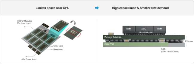
On the computing side, Samsung targets MLCC solutions for GPUs and CPUs that draw hundreds to thousands of amperes at core voltages around 0.8 V. AI accelerators require many more decoupling capacitors than conventional servers while offering less PCB area near the package.
Key strategy elements for the computing segment:
- Push capacitance density:
- Develop ultra‑high‑capacitance MLCCs in very small case sizes (e.g., ≥47 µF in 0402, ≥100 µF in 0603, values according to manufacturer datasheet) for close‑in decoupling.
- Move capacitance closer to the die:
- Promote embedded MLCCs integrated into substrates or packages to reduce parasitic inductance.
- Use landside MLCCs mounted under GPU/CPU packages to exploit the back side of the PCB area.
- Support power integrity at AI transient speeds:
- Shape impedance over a wide frequency range to handle rapid load steps typical of AI workloads.
In practice, this part of the strategy is about turning MLCCs into a tightly co‑designed part of the package–board–VRM system, not just a standard BOM item on the PCB.
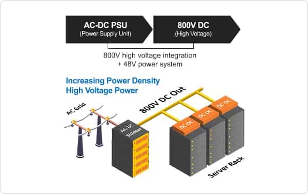
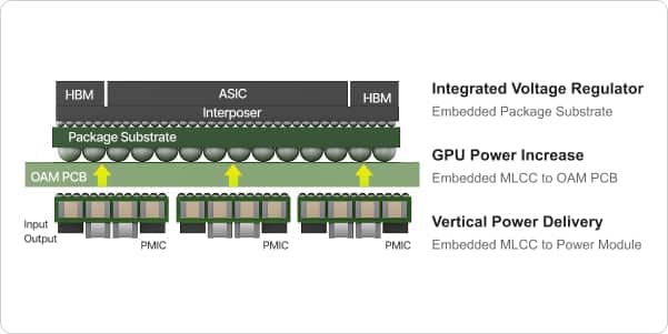
Power: MLCCs for 48 V and 800 V architectures and Vertical Power Delivery (VPD)
For the power segment, Samsung’s strategy follows the shift from legacy 12/48 V conversion schemes to architectures that rectify mains AC to an 800 V DC bus and then convert down inside the rack. As rack power climbs towards the 120 kW class, both efficiency and reliability become critical.
Core strategic directions in power delivery:
- Support higher system voltages:
- Expand 100 V MLCC offerings for 48 V distribution rails to provide robust derating and surge margin.
- Develop large‑size 1 kV–2 kV MLCCs for 800 V DC systems, covering DC link, filtering and snubber roles.
- Enable vertical power delivery (VPD):
- Align MLCCs with VPD modules that shorten the path from VRMs to GPUs, increasing power density.
- Promote high‑capacitance, low‑voltage parts such as X7T 0402 22 µF and X6S 2.5 V 47 µF (under evaluation) as building blocks for VPD decoupling.
- Address thermal and reliability constraints:
- Optimize MLCCs for elevated temperatures and ripple conditions in compact, high‑power PSUs and point‑of‑load converters.
This power‑focused strategy positions MLCCs as enablers of next‑generation rack architectures where efficiency gains at 48 V and 800 V directly impact operating cost and deployment density.
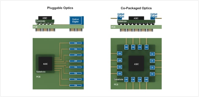
Network: MLCCs for 1.6T switches and co‑packaged optics
On the network side, Samsung’s strategy recognizes that AI clusters are moving to 800G and 1.6T links with co‑packaged optics (CPO), which bring optics and switch ASICs into a single highly integrated module. These network trays have very high power densities and strict signal‑integrity requirements.
Key strategic points for networking MLCCs:
- Address high‑power switch ASICs:
- Design MLCCs for network chipsets consuming more than 500 W in concentrated areas.
- Provide stable capacitance and low loss at elevated local temperatures near the switch and optics.
- Enable co‑packaged optics:
- Support power rails for CPO modules where space, thermal headroom and EMI margins are all tight.
- Tailor MLCCs for placement around high‑speed SerDes and optical engines to maintain power integrity.
- Elevate temperature capability:
- Shift dielectric usage from X5R towards X6S and X7T to support higher operating temperatures in dense network equipment.
- Focus on high‑temperature MLCC product lines for long‑term reliability under sustained load.
In this segment, the strategy connects MLCC development directly to the roadmap of high‑speed networking and optical integration for AI clusters.
Cross-cutting technical themes
Across computing, power and network, several technical themes are common to Samsung’s AI strategy:
- Ultra‑high capacitance density:
- Roadmap targets for tens of microfarads in 0402 and hundreds of microfarads in 0603 sizes for proximity decoupling.
- Higher voltage classes:
- Strengthening 100 V MLCC lines for 48 V racks and expanding 1 kV–2 kV MLCCs for 800 V buses and converters.
- Higher temperature operation:
- Increased reliance on X6S and X7T dielectrics to maintain performance in thermally stressed AI hardware.
- Integration and form factor:
- Embedded and landside MLCC concepts to shorten electrical distances and free top‑side PCB space.
For design engineers and buyers, this means MLCC selection in AI projects will increasingly be tied to system‑level roadmaps for GPUs, power architectures and network fabrics.
Source
This article interprets a Samsung Electro‑Mechanics product news release as a three‑part MLCC strategy for AI hardware, covering computing, power and network segments, and adds system‑level context for engineers and component purchasers.
References
- Samsung Electro‑Mechanics – Strategy for Responding to the AI Industry: Expanding a Three‑Part Series on Computing, Power, and Network
- Samsung Electro‑Mechanics – Component Center / Product Search
- Samsung Electro‑Mechanics – Component Library

