
Supercapacitor balancing system is required to avoid overloading of individual supercapacitor cell in series connection.
Key Takeaways
- Supercapacitor balancing methods prevent voltage overloads in series-connected supercapacitors and ensure longevity.
- The article details both passive and active balancing strategies for supercapacitors, explaining their advantages and drawbacks.
- Passive methods include resistors, Zener diodes, and MOSFETs; they offer lower costs but are slower than active methods.
- Active strategies involve operational amplifiers or DC-DC converters, providing faster balancing but at higher costs and power dissipation.
- Testing showed that each method has unique characteristics, influencing their suitability based on application requirements.
This Würth Elektronik technical article written by René Kalbitz explains some theoretical background of supercapacitor balancing methods and verify it is effectiveness in practical measurement and comparison. Published under Würth Elektronik permission.
Supercapacitors (SC) usually operate at low voltages of around 2.7 V. In order to reach higher operating voltages, it is necessary to build a cascade SC cells. [1] [2] Due to production or aging related variations in capacitance and insulation resistance the voltage drop over individual capacitors may exceed the rated voltage limit. Thus, a balancing system is required to avoid accelerated aging of the capacitor cell. [3] [4].
In the following, we want to explain the effect of unequal voltage division in such cascades in principle. To improve the under-standability we consider a series stack of two capacitors (note: any system may be reduced to an equivalent circuit of two capacitors.). In this note, we review the theoretical background and we provide some measurements as well as discussions on practical examples. The goal is to provide an overview on possible balancing strategies as well as an understanding of the explained concepts. The developer is invited to choose and adapt any strategy to meet specific requirements.
Content
- Balancing Theoretical Background
- Supercapacitors Balancing Strategies
- Measurements
- Summary – What is the Best Supercapacitor Balancing Method ?
Balancing – Theoretical Background
Imbalance of Serial Connected Supercapacitors
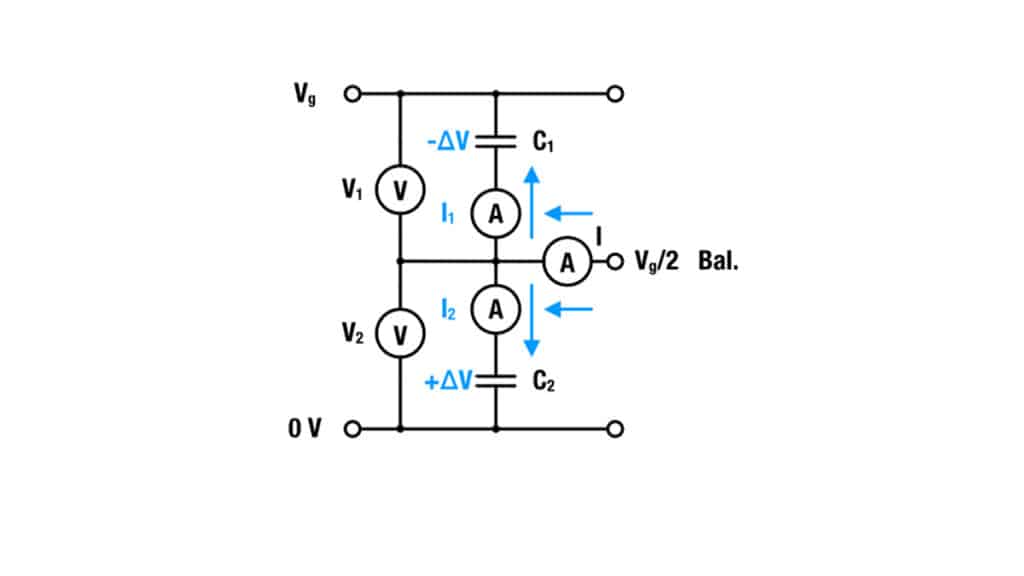
A capacitor may be modeled by a parallel connection of an R-C unit and a insulation resistance. For the moment we neglect the insulation resistance and consider a series stack of two capacitors with capacities C1 and C2 – see Figure 1.

The conserved quantity in such a stack is the condensed charge q at the capacitor, i.e. at its internal interfaces. Using the conservation of charge V1,2 = q/C1,2 the voltage drop over each capacitor is:
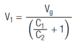
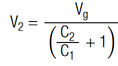
with Vg = V1 + V2 as the total voltage. If both capacitance values are equal, the voltage at the terminals of two serial connected capacitors is equally:
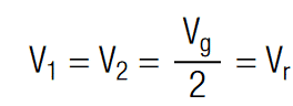
Thus, the system is balanced and each capacitor is charged at its rated voltage Vr. In the following we may consider the case where C1 is larger than C2. With above equations it can be shown that the voltage drop at each terminal is unequal by:
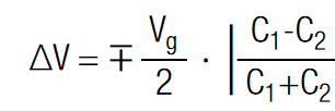
With the voltage difference ∆V, which is in the following referred to as imbalance, we may write:

Using the definition of capacitance C = ∆q/∆V with q as charges at the capacitor interface and V as voltage at the capacitor), the above equation
may be rewritten as:


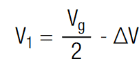
In order to adjust the voltage of each capacitor to Vr = V1 = V2 the charge has to be increased at capacitor 1 and decreased at capacitor 2 by the amount of ∆q. Using the definition of electrical current (I = dq/dt) the voltage may be written as:
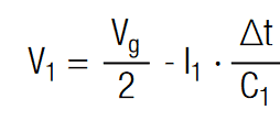
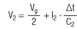
The current I1,2 is interpreted as the electrical current that has to flow for a time period ∆t to equalize this system. The constant current that is required to equalize a voltage difference ∆V in a given time period ∆t is
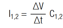
Balancing Current and Balancing Time
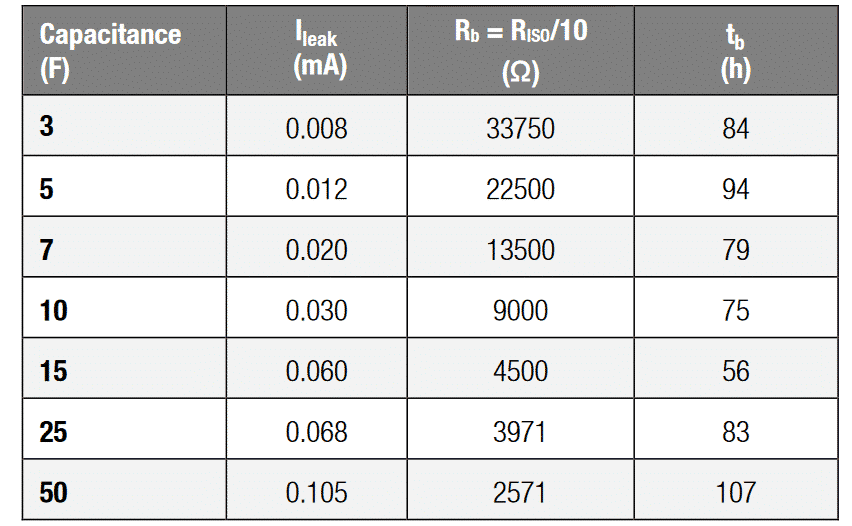
We may use above equations for the estimation of the current magnitude. In this example we used the full tolerance range of the capacitance, which is 40% (-10%/+30%). Hence, for Cr = 10F we obtain C1 = 13F and C2 = 9F. The total voltage of 5.4V provides then a voltage difference ∆V = 0.49V (i.e. at C2 the voltage drop is V2 = 3.19V and at C1 the voltage drop is V1 = 2.21V). The ∆V ≈ 0.5V is the largest possible imbalance. To illustrate this situation, we use the circuit in Figure 1. The balancing current necessary to balance C1 and C2 within 1 sec respectively according to equation [11] are :
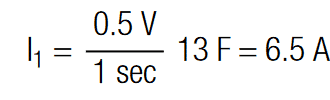
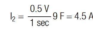
Hence, C1 needs to be charged with I1 = 6.5A and C2 needs to be discharged I2 = 4.5A. The current that has to be provided by the balancing terminal can be calculated with Kirchhoff’s current law. We may consider currents that flow out of the junction as negative and currents that flow into the junction as positive. Since I1 and I2 flow out of the junction and the balancing current I into the junction, the balancing current is:
I = 11A = 6.5A + 4.5A
Although the result may vary depending on ∆V and ∆t this example of calculation may show that balancing at the characteristic RC-time requires currents of several amperes. The balancing current, required to balance a strongly imbalanced system of ∆V = 0.5V ( as calculated above) in within ∆t can be estimated with:

So far we have neglected the insulation resistance, which starts to dominate the electrical behavior as soon as the SC is fully charged and the charging current becomes smaller than the leakage current Ileak. Most manufacturers specify a measurement time of 72h at rated voltage Vr to
determine Ileak. Under these conditions the capacitor may be simply modeled by an ohmic resistance Riso = Vr/Ileak. Hence, if a capacitor is fully charged a serial stack of SC may be considered as a stack of serial connected resistances, which constitute a voltage divider.
Supercapacitors Balancing Strategies
The literature [3,4,6,7,8] categorizes balancing strategies by different properties like:
- energy dissipative behavior,
- balancing speed,
- the type of technology that is used or
- pricing
Thus, when it comes to choosing the right balancing strategy, it is important to now all the parameters and constrains of the specific application to make the right choice. In this note, we distinguish mainly between:
- active balancing and
- passive balancing
Active balancing involves the utilization of actively controlled switches or amplifying systems. [3, 8] Passive balancing utilizes shunts or self-regulating resistors to lower the effect of overvoltage. Compared to passive balancing, active balancing may be fast, in some cases energy efficient but also relatively cost intensive. Passive balancing, on the contrary, is relatively slow, leads to reduction of the charge storing capabilities but it is more cost efficient than active balancing solutions.
Supercapacitors Passive Balancing with Resistors
Figure 2 presents an example of passive balancing with a resistor. The red and green arrows represent the corresponding physical current flow for the case were C1 has either over (+∆V) or under voltage (-∆V). The current for the balancing speed is adjusted (or restricted) by the resistance of the balancing resistors.

The balancing resistors have to meet three main requirements:
- The resistance should be as low as possible to allow a fast balancing. This will be beneficial for the lifetime.
- The resistance should be as high as possible to minimize losses and minimize the self-discharge.
- The accuracy of the resistors/shunt should be sufficient (≤ 1%) in order to provide an accurate reference.
Clearly, it is necessary to find an optimum between short balancing times and low self-discharge. The balancing resistance would have to be the order of the equivalent series resistance RESR, to balance the supercaps within the characteristic RC-time. This is a theoretical consideration and not practical, since it would mean we permanently short-circuit the SC. A good rule of thumb is one tenth of the insulation resistance, i.e.

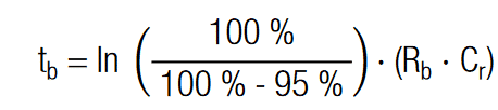
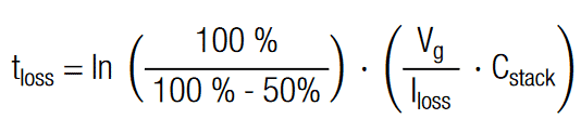
With Vr as rated voltage and Ileak as leakage current (both values are given in the data sheet of the SC). Due to its magnitude, Rb balances differences in insulation resistances. The maximum current that can flow at ∆V is Imax = ∆V/Rb. The time to equalize a imbalance ∆V up to 95 % can be calculated with:
which can be well approximated with:
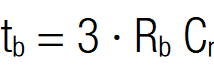
The resulting balancing times, given in Table 1, are indeed in the range of days. With the given balancing resistances, the self-discharge rate per day is about 41 %. Thus, for many power applications the resistance may even be reduced, at the expense of charge storing abilities and balancing speed.
Supercapacitors Passive Balancing with Zener Diodes
An improved balancing time can be achieved, if the resistor is replaced by a Zener Diode as indicated in Figure 3. The arrows again indicate the electrical current flow, in case of a imbalance. The Zener diodes constitutes a variable resistor or a voltage dependent switched resistor. Since the internal resistance is reduced at the breakdown voltage, it is possible to drastically reduce the balancing time in comparison the linear resistor.
Diodes may also serve as general protection against reverse polarity. Especially for larger stacks, it can be advisable to place Zener diodes in parallel to metal oxide semiconductor field effect transistors (MOSFET). The accuracy of the breakdown voltage is, compared to the accuracy of ohmic resistors, usually relatively low. In total the tolerances could be as high as around 10 %.
Possible overvoltages could be still avoided by a reduction of working voltage. For operations at higher temperatures, it might also be necessary to consider the shift of breakdown voltage due to the temperature coefficient.
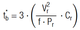
The strong voltage dependence of the reverse current makes it difficult to calculate the balancing time accurately.[8] The actual current characteristic of commercial Zener diodes are often not given in the datasheet. It is however possible to roughly estimate the balancing time on the basis of the above expression for tb (see previous section) A rough estimate can be made with the rated power dissipation of the Zener diode Pr, usually given in the datasheet. If the diode breakdown voltage is equal to actual operating voltage, VR we may substitute Rb* = Vr2 / Pr into above expression for tb and with f as correction factor we obtain:
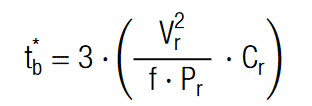
Due to the strong voltage dependence of the reverse current, it may be necessary to adjust f from case to case to its effective value. Since the diode will most of the time operate well below its total power dissipation we suggest f = 1/10.
Supercapacitors Passive Balancing with MOSFETs
Another type of balancing can be utilized with a MOSFET as given Figure 4. Similar to the Zener diode, the MOSFET constitutes a voltage driven switch or variable resistor.
The arrows again indicate the electrical current flow, which is similar to the passive balancing in Figure 2. As soon as the voltage imbalance exceeds the threshold voltage of the MOSFET, the increased drain voltage leads effectively to a discharge of the overcharged capacitor. It is possible to think of the MOSFET as voltage dependent resistors, which leads to improved balancing times compared to passive resistors.
Supercapacitors Active Balancing with Operational Amplifier
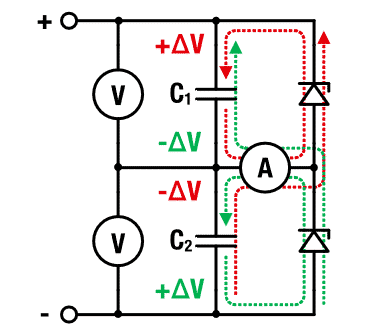
Any application that needs a shorter balancing time will have to apply an active balancing. Active balancing always involves integrated circuits such as operational amplifier (OP-AMP), which is illustrated in Figure 5. The circuit contains red and green arrows, which represent the corresponding physical current flow for the case were C1 has either over (+∆V) or under voltage(-∆V).
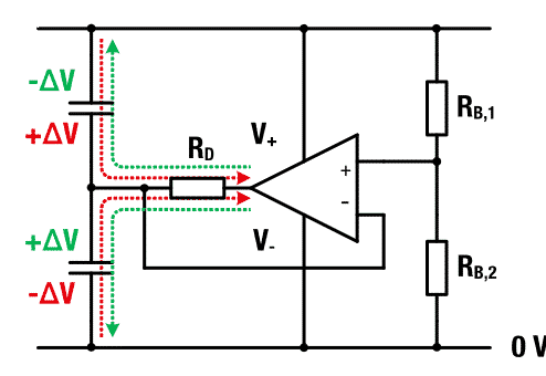
The balancing resistance, as used for the active balancing, is determined on the basis of the designated internal resistance of the OP-AMP, which is at least the order of 10 MΩ but usually even higher. To ensure the voltage detection at the inputs the balancing resistances RB,1 and RB,2 should be about 10 times smaller than the internal resistance of the OP-AMP. As a result, the loss through the balancing resistance can be as small as for the internal resistance of the SC.
However, a more significant cause of loss is the supply current, delivered through contacts V+ and V -. Depending on the type of OP-AMP the permanent supply current may be in the range from 1μA to 10mA. This may pose a technical obstacle, that needs to be considered at the conceptual design-in phase. The balancing current is provided by the output of the OP-AMP and regulated via the feedback loop. The damping resistance RD at the output of the OP-AMP is only as high as to prevent oscillation during the current regulation.
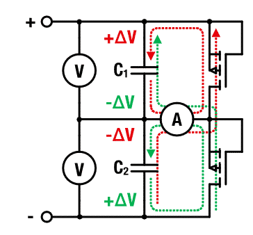
Supercapacitors Active Balancing with DC-DC converter
Another concept of active charge equalization consists of DC-DC converters, each connected across two neighboring cells, as illustrated in Figure 6. Due to the low losses of commercially available converters, this concept is in terms of balancing time and power burn more efficient than passive balancing.
There are balanced buck-boost SC chargers available on the market, which are suitable for a range of applications. Available for instance are Analog Devices:
- LTC3351, Hot Swappable Backup Supercapacitor Charger
- LTC3128, Supercapacitor Charger and Balancer
Additional information are also provided in the Würth Elektronik (WE) Webinar “WE Backup Your Application – A real life SC backup solution”.[11]
Although DC-DC converters constitute a relatively costly balancing strategy, they are on the other side also an elaborate and comprehensive solution. They may provide complete charging and hot swappable charging solutions with low power consumption. The choice at the end is always with the developer.
Measurements
The voltage measurements were performed with a self-developed measurement setup, based on the integrated circuit CY8CKIT-059 from PSoC. The data acquisition was utilized with an Excel-script. The measurement setup including the programming of the script were developed by Jon-Izkue Rodriguez from WE eiSos.
The power supply we used was the HMP4040 from Rohde & Schwarz. The currents for the determination of the power dissipation were measured with M252A METRAHit ESPECIAL Current Transformer Connection Multimeter from Gossen-Metrawatt.
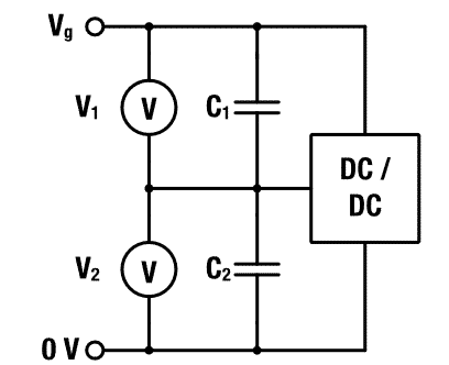
We tested a series combination of two SC from WE eiSos
- Capacitor 1: C1 = 10 F
- Capacitor 2: C2 = 15 F
This practically constitutes deviations from a theoretical capacitor with a rated capacitance of Cr = 12.5F. For the charging we used a
- charging voltage Vg = 5.4V
- max. charging current Ic = 2A
For the sake of reliable circuit design, we want to underline that combining SC with different rated capacities is inadvisable. We only choose this combination for experimental purposes. This setup provides three advantages:
First, this set up provides a significant and reproducible imbalance of around ±0.5 V. We could change the set of capacitors without an intensive search for suitable mismatches. Second, it also demonstrates the potential robustness of the EDLC, if operated under extreme overvoltage. Although the lifetime were drastically reduced to few weeks, none of the used SC showed a catastrophic failure. Third, it shows the operation of the individual balancing strategies under extreme conditions.
The chosen capacitors demonstrate the operation of each strategy under extreme imbalance. In practice, the variation of capacitance is much lower than in this example, even over different production batches. We also studied the self-discharge behavior of each circuit for a period of 24 h. Hereunto, we disconnected the entire balancing circuit from the primary power source after the capacitors were fully charged and balanced. The voltage was again measured with the PSOC CY8CKIT-059.
Based on the measurements we also give an assessment about the applicability of the circuit in stand-alone long-term applications. In that respect, the expression “long-term” describes a period of approximately several days.
Resistor, 1 kΩ Passive Balancing
For the passive balancing, as shown in Figure 2, we used a 0.6 W, 1kΩ (1%) resistance. We have chosen the resistance in favor of a short balancing time rather than a low power loss. The measured voltages V1 and V2 and the resulting voltage difference |V1 – V2|, given in Figure 7, show a complete balancing after around 600 min. V1 and V2 approach Vr asymptotically.
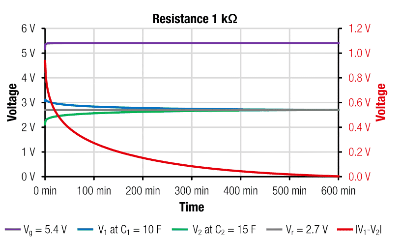
The measured balancing time corresponds to the estimation, given in section 4.1, tb = 625 min = 3 ∙ Rb ∙ C = 3 ∙ 1 kΩ ∙ 12.5F. The overall power dissipation (effective leakage current, Iloss) after 12h is 2.8mA ∙ 5.4V ≈ 15 mW. For low power applications or for backup solutions this balancing speed may be sufficiently fast and the power loss is acceptable. For battery driven (standalone) applications, the resistance should be increased to reduce losses. To be on the safe side, it is also advisable to reduce operating voltage, to avoid overvoltage. The half-life, self-discharge time is estimated with:
Hence, in this example:

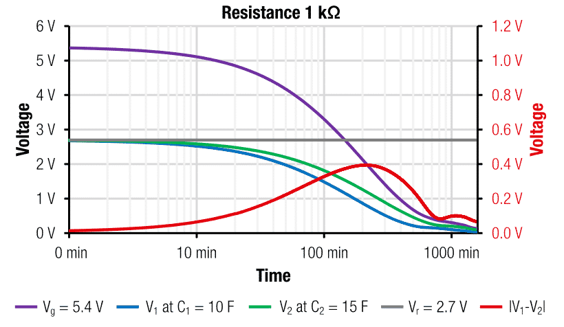
The results of self-discharge measurement as given in Figure 8 correspond to the estimated half-life self-discharge time of around 130min. The self-discharge time is large enough to consider passive balancing with 1 kΩ as suitable for a standalone solution.
Zener Diode Passive Balancing
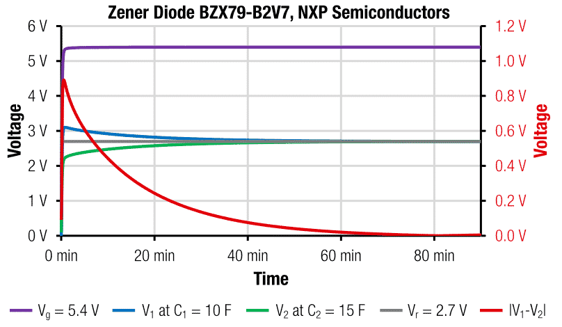
For the passive balancing, as shown in Figure 3, we used the voltage regulator diodes BZX79-B2V7 from NXP Semiconductors. The results, given in Figure 9, indicate a complete balancing after around 80min. With the datasheet value of total power dissipation of 500mW, the measured value fits roughly to the theoretical approximation of:
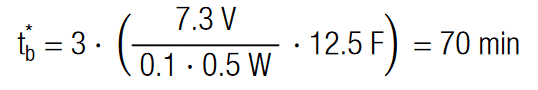
The overall power dissipation (effective leakage current, Iloss) after 12h is 5mA ∙ 5.4V ≈ 27mW. For lower voltages the power dissipation will be even lower. (The datasheet states: Iloss(1V) = 20μA).
Due to the strong nonlinear voltage dependence of Zener diodes, the calculation of the self-discharge characteristic is difficult. We may however use the same concept as for tb* and introduce a correction factor f to adjust the expression for the half-life self-discharge time. We may estimate that the data sheet value Iloss (1V) = 20μA is in our case about 10 times higher. With f = 10 the theoretical half-life self-discharge time for a stack, balanced with a Zener diode, can be estimated with:
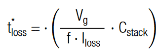
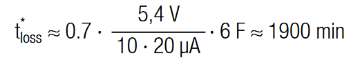
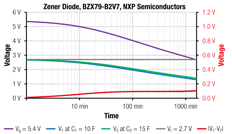
The results of self-discharge measurement, as given in Figure 10, show that tloss* = 1900min roughly fits the actual half-life self-discharge time. Based on the measured self-discharge behavior, we think, the circuit could still be suitable for long-term stand-alone applications.
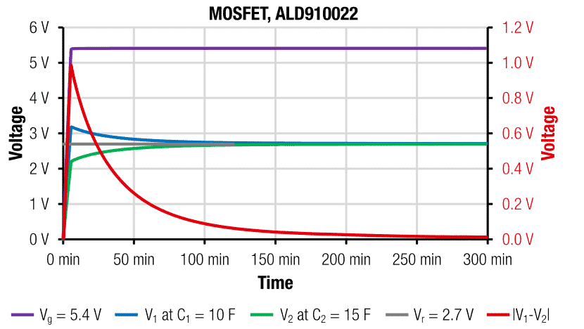
MOSFET Passive Balancing
The MOSFET based balancing circuit, as given in Figure 4, was implemented with the test board SABMB2 for the MOSFET ALD910022 (Test Board SABMB2) from Advanced Linear Devices. The results in Figure 11 indicate a complete balancing after around 300min. The overall power losses after 12h of 1.5mA ∙ 5.4V ≈ 8mW were about as low as for the Zener diode.
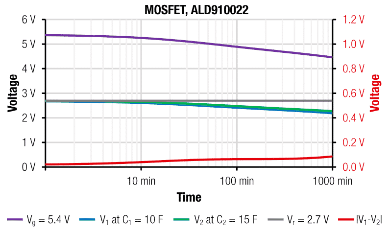
The results of the self-discharge measurement in Figure 12 show that after 24h the total cell voltage has decreased to about 4V. With this rate tloss will be in the order of several days. A comparison to the maintain voltage measurement at the REDEXPERT online tool [10] suggests that the MOSFET does not significantly increase the self-discharge rate. We therefore conclude the circuit is suitable for long-term stand-alone applications.
Amplifier Active Balancing
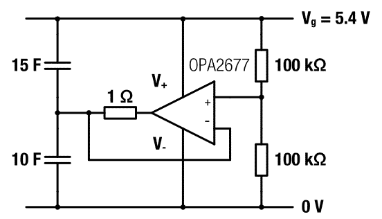
For the active balancing with the amplifier OPA2677 (Texas Instruments), we utilized a circuit as given in Figure 13. The advantage of the OPA2677 is the relatively high output current of 500mA, which enables a fast balancing.
The measured cell voltages in Figure 14 show an instantaneous balancing within the charging time, which is in this measurement about 3min. The balancing speed can be further increased by decreasing the damping resistor from 1Ω to 0.4Ω. With 0.4Ω the balancing times of around 2min were reached. The trade of was a noticeable decaying oscillating behavior. The damping resistor at the output should not be below 0.4Ω to prevent oscillation of the output voltage. We found 1Ω to be the optimum between fast balancing and damping.
The overall power dissipation after 12h is 50mA ∙ 5.4V ≈ 270mW. The power is manly dissipated via the supply terminals of the amplifier. This relatively high power consumption shows the main disadvantages of this type of strategy. It is fast but it also has a large permanent power burn.

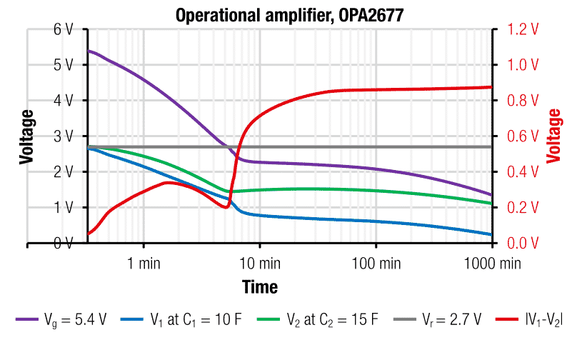
The results of the self-discharge measurement in Figure 15 indicate a half-life self-discharge time of tloss = 5min. Since we may only speculate about the voltage dependence of current losses at the terminals, we refrain from a mathematical estimation of tloss. We do not consider the circuit suitable for long term standalone application.
Although the circuit always ensured a balanced charging, the losses via the supply channels are significant. We demonstrated, however, the feedback amplifier might work in principle. It is at the end the developers responsibility to find the best solutions for his application.
Active Balancing with DC-DC Converter
The evaluation board DC1887A utilizes the buck-boost SC charger and balancer LTC3128 from Analog Devices. It is charging the SCs at a preset voltage of 4.2V. The board operates at a supply voltage of 5.5V. The measurement results, given in Figure 16, indicate a complete balancing after 1.5min. The overall power dissipation after 12 h is 0.1mA ⋅ 5.4V ≈ 0.5mW.
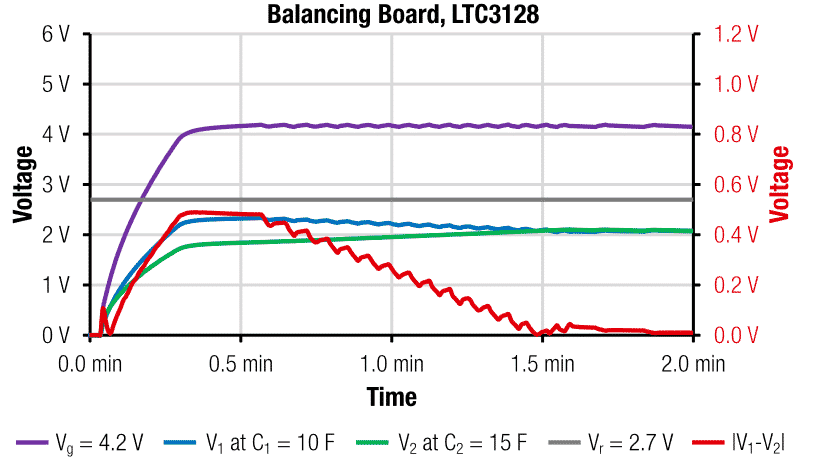

The measurement results of the self-discharge in Figure 17 show that after 24h the cell voltage has decreased from 4.2V to about 3.4V. With this rate tloss will be in the order of several days. Thus the SC charger and balancer LTC3128 is suitable for long term standalone applications.
Summary – What is the Best Supercapacitor Balancing Method ?
We have reviewed the theoretical description of active as well as passive balancing strategies and performed some practical measurements to illustrate the different characteristics of each strategy.
In the following, we assess the tested balancing circuits on the basis of balancing speed, power dissipation as well as pricing. It is however, the responsibility of the developer to find the best solution based on even more comprehensive parameters. Availability, lifetime and design-in time might also influence the choice of balancing strategy.
The balancing with the resistor is the slowest balancing strategy, but yields the advantage of low power consumption, low cost and easy circuit design. Depending on the resistors it might be suitable for long-term standalone applications. The balancing speed of the Zener diode is moderate. It yields the advantage of relatively low power consumption, low cost and easy circuit design. The relatively low power dissipation makes it suitable for long term standalone applications.
The MOSFET circuit showed a relatively low power dissipation. Its balancing speed of the given example is moderate. We found the MOSFETS might be suited for long term standalone applications. The OP-AMP certainly provides a fast balancing in comparison to the other strategies, but shows the largest power dissipation. Compared to the other strategies it constitutes the most expensive solutions. Due to the high power dissipation, it may not be suitable for standalone applications.
The balancing DC/DC board provided the fastest balancing and a moderate power dissipation. It is generally an overall convenient but somewhat pricey solution. Concerning the included DC/DC conversion, its overall cost can be considered as moderate. Due to its low power dissipation, it might be suitable for long-term standalone application.
An overview of the summarized results is given in Table 2.

FAQ: Supercapacitor Balancing Methods
Balancing is necessary when supercapacitors are connected in series to prevent individual cells from exceeding their voltage limits due to differences in capacitance and insulation resistance, which can lead to accelerated aging or failure.
There are two major types: passive balancing (using resistors, Zener diodes, and MOSFETs) and active balancing (using operational amplifiers or DC-DC converters). Passive methods are simpler and lower in cost but slower, while active methods are faster and more efficient, though generally more expensive.
Passive resistor balancing equalizes voltage across series-connected supercapacitors by shunting excess charge through resistors. It is simple and cost-effective but relatively slow and can cause increased self-discharge rates.
Zener diode balancing uses voltage-dependent diodes as shunt elements, providing faster balancing than resistors, with moderate power dissipation, and better overvoltage protection, though tolerance can vary.
MOSFET balancing acts as voltage-dependent switches that rapidly discharge overcharged cells, achieving moderate balancing speed and low power dissipation. Suitable for long-term, stand-alone applications.
Active balancing (e.g., using operational amplifiers or DC-DC converters) is recommended when fast balancing and low power loss are critical. These solutions are ideal for applications requiring frequent or rapid charge equalization, despite higher cost.
The best balancing method depends on required speed, cost, power efficiency, and application specifics. Passive resistor solutions excel in low-cost, long-term stand-alone setups; Zener and MOSFETs provide a balance between speed and efficiency; active solutions offer the fastest balancing but at higher expense and complexity.
How-To: Choose and Implement Supercapacitor Balancing Strategies
- Define your application requirements
Decide if your system needs fast balancing, low power loss, cost efficiency, or is intended for long-term stand-alone use.
- Select a balancing strategy
Choose passive resistors for simple, low-cost solutions. Opt for Zener diodes or MOSFETs if you require moderate speed and low power loss. Use active balancing with operational amplifiers or DC-DC converters for rapid and precise balancing.
- Calculate component values
For passive balancing, select resistor values balancing speed with self-discharge (generally one-tenth of insulation resistance). For Zener/MOSFET, refer to datasheets for voltage thresholds.
- Assemble and test
Build the chosen balancing circuit. Monitor voltage across each cell and measure self-discharge rates. Adjust component values for optimal performance.
- Maintain and optimize
Periodically check cell voltages and balancing performance, replace aging components as needed, and tune the system as your requirements evolve.
Literature
[1] F. Beguin und E. Frackowiak (Hrsg.), Supercapacitors Materials, Systems, and Applications, WILEY-VCH Verlag, ISBN: 978-3-527-32883-3, S.352ff (2013)
[2] R. Kötz et al., Principles and applications of electrochemical capacitors, Electrochimica Acta, 45 (15-16), 2483-2498, doi: 10.1016/s0013- 4686(00)00354-6 (2000)
[3] D. Linzen et al., Analysis and Evaluation of Charge-Balancing Circuits on Performance, Reliability, and Lifetime, of Supercapacitor Systems. IEEE-
Transactions on Industry Applications, 41(5), 1135-1141, doi: 10.1109/tia.2005.853375 (2005).
[4] H. Li et al., Synchronized Cell-Balancing Charging of Supercapacitors. IFAC-PapersOnLine, 50(1), 3338–3343, doi:10.1016/j.ifacol.2017.08.518 (2017)
[5] R. Kalbitz et al., Supercapacitor – A Guide for the Design-In Process, Application Note ANP077, WE eiSos (2020)
[6] Y. Qu et al., Overview of supercapacitor cell voltage balancing methods for an electric vehicle, 2013 IEEE ECCE Asia Downunder, doi: 10.1109/ecce-asia.2013.6579196 (2013)
[7] F. M. Ibanez, Analyzing the Need for a Balancing System in Supercapacitor Energy Storage Systems, IEEE Transactions on Power Electronics,33(3), 2162-2171, doi: 10.1109/TPEL.2017.2697406 (2018)
[8] B.T. Prashant Sing et al., Extensive review on Supercapacitor cell voltage balancing. E3S Web of Conferences. 87. 01010.10.1051/e3sconf/20198701010 (2019)
[9] K. B. McAfee et al., Observations of Zener Current in Germaniump−nJunctions, Physical Review, 83(3), 650–651. doi:10.1103/physrev.83.650 (1951)
[10] Link to Supercapacitor Modul in REDEXPERT
[11] Link to Online-Seminar “WE Backup Your Application – A real life Supercapacitor backup solution”
Other article on supercapacitor active balancing evaluation was presented during PCNS Passive Components Networking Symposium 2019: Evaluation of Active Balancing Circuits for Supercapacitors

