
Dennis Zogbi, Paumanok Inc. publishes on TTI Market Eye overview of thin film integrated passive devices, its materials and processes and presents its potential to boost component volumetric efficiency.
Introduction
Thin film integrated passive devices combine those latest solutions for volumetric efficiency in modules, chipsets and chiplets, and this originates in their precise engineering and the enhanced compactness they afford design engineers.
Moreover, as economies of scale drive down prices, these advanced technologies are becoming increasingly accessible, emerging from their specialty verticals in high-reliability markets toward modules and chipsets for mass production in consumer, communication and computer end use market segments.
This article describes the component and materials trends and directions leading the way for the next installment of volumetric efficiency in passive electronic components.
Historical Development, Technology, Types and Configurations
In the 1960s, resistor manufacturer pioneers began to package individual resistors into single-in-line packages (SIP) that housed from four to eight individual components. This packaging reduced the cost to “pick and place” resistors on a printed circuit board (“conversion cost”).
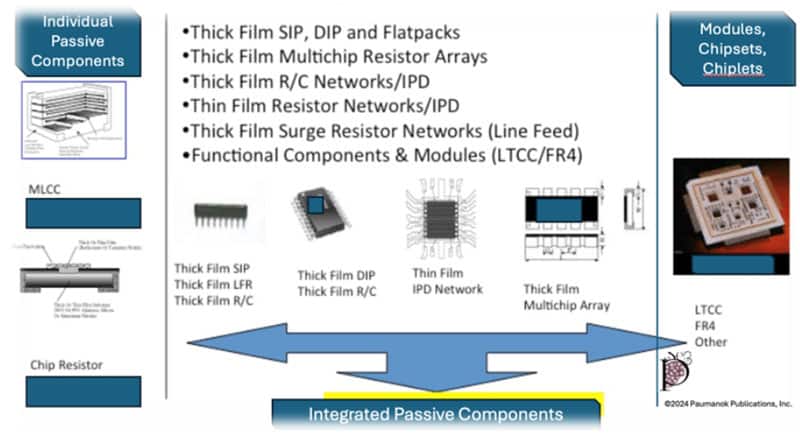
Soon after, the component manufacturers realized that their ability to make resistor networks on an alumina bridge also meant that they could provide value added configurations (such as bussed and R2R ladder circuits for filtering and line-termination). Over time, this concept was enhanced to include thick-film networks of 16 to 32 resistive elements within dual-in-line packages in plastic housings with gull-wing leads for easy surface mounting. The dual-in-line package made it possible to for resistor manufacturers to integrate different types of passive components, usually chip resistors and ceramic chip capacitors.
Semiconductor Processes Applied to Passive Components
In the early 1990s, new developments in passive component configuration were pioneered by early settlers in the semiconductor industry. These companies used semiconductor manufacturing techniques to manipulate specific raw materials, such as tantalum nitride, chrome silicide and nickel chromium to create layers of resistance. They also used ion-implantation devices to engineer silicon-oxide and silicon-nitride capacitors, thereby creating complex integrated passive devices, which in theory and practice extend the realm of volumetric efficiency by creating whole circuits such as filters or power amplifiers.
Additional silicon manipulation in thin film added transistor functions and circuit protection functions to integrated passive devices. The new thin film-on-silicon designs began to compete against traditional thick-film DIPs and SIPs for termination and filtering functions, especially in high frequency applications (see Figure 2 below). This new movement for advancing volumetric efficiency in electronic sub-assemblies combined both advanced thin film semiconductor processing techniques with advanced resistive, capacitive and inductive metals with FR4 plastic, ceramic and silicon substrates. This is considered disruptive technology because it upsets the thick film pick and place insertion solution for mass produced electronic components.

New Materials for Resistors, Capacitors and Inductors for Thin Film Solutions
Thin films are used in network designs when more precise resistance values are required or where volumetric efficiency is a primary concern. Minor market movers include moisture and pollution resistance of thin films in passive components as well. The processes and materials required for thin film integration of passive components differs, making each function challenging to integrate. Resistance is accomplished with a masking tool, capacitance is accomplished with an ion implantation tool and inductance is accomplished through line deposition.
Each basic functionality can be achieved but at a high price because of the capital equipment costs associated with each step. Individual passive components (MLCC, Chip R, Ferrite beads) and their packaged configurations (Array, SIP and DIP) will remain cost effective in comparison to thin film solutions for the foreseeable future and will only slowly gain new ground in mission critical applications where the needs for volumetric efficiency, precision performance, moisture resistance and/or chemical resistance are design parameters.
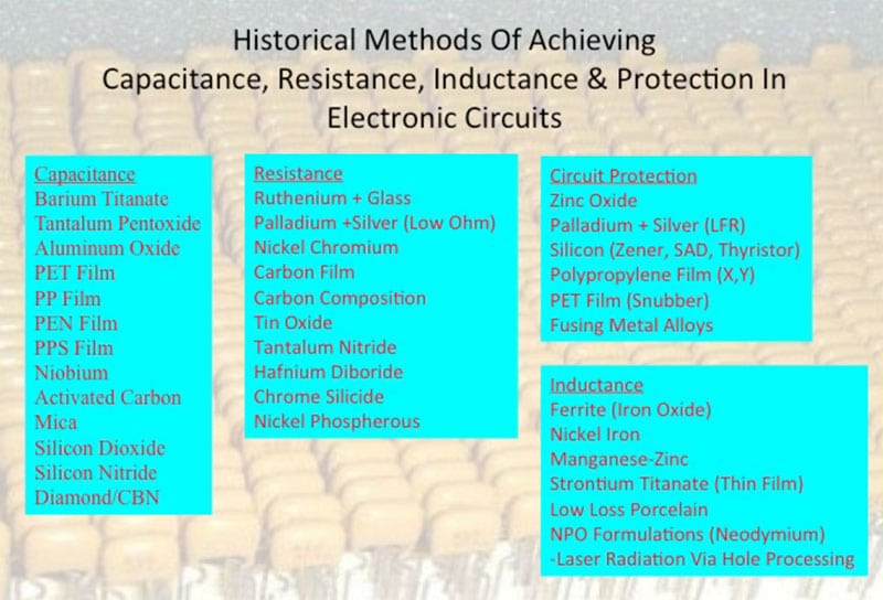
Thin Film Resistance: Thin-film resistors are currently manufactured using sputtering targets manufacturing from such materials as nickel-chromium, tantalum-nitride, chrome-cobalt, hafnium diboride, nickel phosphorous, and chrome-silicide.
These thin film resistor materials are deposited or “sputtered” on ceramic substrates using physical vapor deposition of metal “targets.” This process is a legacy semiconductor manufacturing technique which is dissimilar to the traditional method of mass-producing capacitors, resistors and inductors, which is largely ceramic and metal based and involves titanates, alumina, tantalum, plastics and mixed metal alloys.
Thin Film Capacitance: Meanwhile, in capacitors, the traditionally need for “charge on call” is satisfied by the multilayered ceramic chip capacitor, which is largely based upon titanate ceramics and related chemistries. If the silicon is removed from the equation, we see that ceramics occupy a large volume of space on the printed circuit board. These multilayered ceramic chip capacitors (MLCC) are further manufactured from a recipe of interleafing ceramic and metals, with a keen reliance on nickel and copper but also palladium and silver in the specialty markets where thin film currently competes. With an eye on Industry 4.0 and Work 5.0 transparency initiatives, design engineers have considered using ion implantation techniques to implant silicon capacitors – nitride or silicon dioxide capacitors in close proximity to the active component that needs their charge.
Moreover, significant strides have been made in the development of silicon trench capacitors, where the precise ability to stack silicon materials have shown capacitance values in excess of 1 microfarad. Some of the more successful work in developing silicon capacitance has been captive by companies who manufacture semiconductor modules, chipsets and chiplets. Added benefits are noted by extending the silicon to include rectifiers, Schotzky diodes and transistors.
Thin Film Inductance: Thin film inductors are also being manufactured that employ barium strontium titanate dielectric thin film materials to create nanohenry values in integrated passive devices. There is also the ability to print thin film coils using trace lines of mixed metal alloys. Additional materials and processes for the creation of magnetics is noted in the chart below.
Impact on Module, Chipset and Chiplet
The ability to create thin film resistance, capacitance and inductance has thus far impacted the module, chipset and chiplet markets which feed into other large industries. This snap-in “turn-key” module solution is important for volumetric efficiency and increased throughput of manufacturing for the future of handsets and other portable electronics as well as for individual nodes for telecommunications and data-communications backbone equipment. There are also mission critical programs in civil aviation, satellites, medical implants and portable scanners that employ integrated passive devices and advanced solutions for the digital watch and personal health monitoring industry markets worldwide.
Synergistic Technology Platforms in Thin Film Passive Component Integration
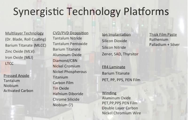
The materials noted in Figure 3 and their sourcing, engineering, application and processing will be key to moving technology forward over the next 100 years with respect to increasing volumetric efficiency of modules and end products. A combination of thick and thin film will continue to command the global market, but over time thin film will gradually win more slots in high frequency applications and in power and communications markets where volumetric efficiency is a design parameter that changes constantly.
In addition to specific materials and their thin film properties, the processes for these materials come into play when cost is considered. The costs associated with manufacturing traditional capacitors, resistors and inductors are much lower than the costs associated with thin film semiconductor manufacturing. Semiconductor manufacturing equipment is in fact much more expensive per machine than an entire ceramic capacitor production facility.
Certain passive electronic component technology platforms have synergies (see Figure 4), and certain materials lend themselves to these processes and have tech data support and 50-year real world application data. A major brand name customer noted that they needed to begin to branch out and learn more about varying materials to expand their comfort zone beyond the usual boxes on the period table. Design engineers of the future will require a greater knowledge of numerous materials and process steps to create components that are “practically invisible, precise in their operation from lot-to-lot and integrated with other components.” To that end, the following chart (Figure 4) illustrates seven methods of increasing volumetric efficiency in individual component production, largely driven by demand from modules, chipsets and chiplets.
Summary and Conclusions: Insights into Next Generation Volumetric Efficiency
We estimate that a combination of unique and advanced materials and semiconductor processing techniques will move technology forward with respect to volumetric efficiency, a cornerstone trend for portability and transportation.
In addition to the ongoing technology trends in individual component miniaturization and advanced function level packaging in modules, chipsets and chiplets, there are key trends emerging in integrating these materials and processes to create smaller parts with greater performance characteristics.
One key vision for manufacturers of components and modules is that through new practices of Industry 4.0 and Work 5.0 initiatives requiring greater visibility on supply chains and the impact of support components on corporate and national sustainability goals, there is a movement toward 100% etched, stacked or ion implanted silicon solutions or sputtered ceramics or metals.
Using these materials, all capacitor, resistor and inductor functions, as well as added functions such as sensing and protection can all be produced with semiconductor manufacturing equipment and related process steps in masks and ion implantation. This creates a new vision for ultra-small modules, chipsets and chiplets related to volumetric efficiency and passive component integration.

