Electromagnetic compatibility (EMC) is decided in the schematic and layout, not in the test chamber. This article distills key lessons from a Würth Elektronik webinar on EMC with electromechanical connectors, focusing on return paths, coupling mechanisms, connector usage and passive components so design engineers and purchasers can build systems that pass EMC with fewer iterations.
The Würth Elektronik webinar walks through how fast digital edges, parasitics, PCB layout and connectors interact to create or mitigate EMC issues, using practical examples that map directly to real‑world hardware development.
Key Takeaways
- Electromagnetic compatibility (EMC) relies on design decisions made during schematic and layout, not just testing.
- Fast digital edges and parasitics greatly affect EMC behavior; shorter rise times increase challenges.
- EMC issues stem from coupling mechanisms like capacitive, inductive, and impedance coupling; understanding these helps in mitigation.
- Layout and return path control are crucial; maintaining low inductance and minimizing interference can boost EMC performance.
- Component selection should prioritize signal integrity and empirical data to avoid EMC failures in high-speed applications.
Key concepts: signals, rise time and EMC
Fast digital interfaces are often described only by their bit rate or fundamental frequency, but EMC behavior is driven by edge speed and harmonics rather than nominal clock alone. A square wave with the same fundamental frequency but shorter rise and fall times requires far more bandwidth to transmit, because its spectrum contains many higher‑order harmonics. Reducing rise time by a factor of 10 roughly increases EMC challenges and transmission‑line constraints by a similar factor, which is why jumping from USB 2.0 to USB 3.x is so demanding for layout and interconnects.
A useful mental shift is to stop thinking purely in a DC universe where current seems to move nearly instantaneously from source to load. In reality, the average drift velocity of electrons in a conductor is extremely low, while the electromagnetic field propagates near the speed of light via the parasitic capacitances and inductances of the circuit. This is why a lamp can begin to turn on in nanoseconds even though electron drift is slow: the transmission line and load are charged through parasitic elements long before individual electrons traverse the entire cable.
The same effect means that even an “open” cable temporarily carries current: when a fast transition is applied, the line charges until the wavefront reaches the unterminated end and is fully reflected, causing characteristic transient peaks on ground and adjacent traces. For EMC, the takeaway is that every interconnect behaves as a transmission line during fast edges, and your layout must anticipate this behavior.
Rise time vs. EMC impact
| Interface example | Approx. fundamental | Relative rise time | EMC / layout implication |
|---|---|---|---|
| USB 2.0 | 240 MHz | 1× (reference) | Easier to route, fewer EMC issues if layout is decent |
| USB 3.x | Same fundamental | ~10× faster | Far more harmonics, EMC issues roughly scale, stricter layout and interconnect requirements |
Coupling mechanisms and field regions
EMC problems are essentially about unwanted coupling between parts of a system. The webinar distinguishes three coupling types:
- Capacitive (electric‑field) coupling
- Inductive (magnetic‑field) coupling
- Impedance/galvanic coupling via shared return paths
Overview of coupling mechanisms
| Coupling type | Dominant field | Typical symptoms | Mitigation approach |
|---|---|---|---|
| Capacitive | Electric | High‑impedance, high voltages | Conductive shielding tied to solid reference |
| Inductive | Magnetic | Low‑impedance, unwanted current | Minimize loop area, use ferrites / metal enclosures |
| Impedance / galvanic | Mixed | Shared return path noise | Separate returns, control return‑path geometry |
In the near field, either the electric or magnetic component of the field dominates, depending on source and geometry. Electric‑field dominated coupling tends to involve high impedance and high voltages; magnetic‑field dominated coupling tends to involve low impedance and significant unintended currents. In the far field, the field ratio approaches the characteristic impedance of free space, about 377 Ω, and conventional antenna theory applies.
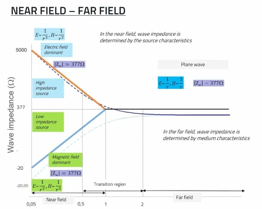
A practical rule of thumb for far‑field behavior is to consider distances greater than approximately one wavelength from the source. For example, at 30 MHz the wavelength is about 10 m, which also matches typical antenna‑to‑equipment distances in radiated EMC measurements. For most design work, it is sufficient to differentiate between the near field and the far field and to treat the mathematically complex transition region as an academic detail.
Capacitive coupling is generally easier to control by adding conductive shields tied to a solid reference. Magnetic coupling is harder: it is mitigated by loop minimization, careful routing, spacing and, where justified, high‑permeability materials such as ferrite sheets or metal enclosures. Impedance or galvanic coupling arises when multiple signals share a return path, allowing noise currents to modulate sensitive circuits, which is often the root cause of unexpected EMC failures.
Layout concepts and return‑path control
A central theme of the webinar is that every conductor and plane forms a transmission line and must be designed with its return current in mind. At low frequency, current returns along the path of least resistance; at higher frequencies, it follows the path of least impedance, which is typically directly under or adjacent to the forward trace on the reference plane. This configuration lets opposing magnetic fields partially cancel, lowering the loop area and radiated emissions.
When the return path is interrupted by slots, cut‑outs, or split planes, the current is forced into large detours that create sizeable loops. These loops are “EMC volcanoes” visible in near‑field scans: regions where strong magnetic fields appear because the forward and return currents no longer cancel. In galvanically isolated flyback converters with separate primary and secondary ground planes, capacitors between grounds can provide controlled RF return paths, but in safety‑critical domains such as medical equipment, such capacitors may be restricted and other strategies are needed.
Near‑field scanning systems, such as EMC visualization benches with built‑in sensor grids, make these issues visible by mapping local magnetic fields above the board. Experiments show that areas with tightly coupled forward and return paths exhibit very low field strengths, while regions with plane interruptions or large loop areas show high peaks.
A few practical measures emphasized in the presentation:
- Keep high‑di/dt loops physically small and on layers with solid reference planes.
- Avoid splitting return planes under high‑speed or noisy traces.
- Where plane splits are unavoidable, provide controlled high‑frequency return paths (for example, capacitors between reference regions where allowed).
- On multilayer boards, prefer stackups where signal layers are immediately adjacent to ground or power planes, not separated by other signal layers.
Via usage, parasitics and filter performance
Parasitic inductance and capacitance are unavoidable but can be managed. Even details like via count and thermal reliefs contribute to the total parasitic network that shapes EMC and filter performance.
Simulations in the webinar compare single‑via versus multi‑via connections between pads and planes. Moving from one via to three vias at a pad can reduce effective stray inductance by roughly a quarter, which directly improves the attenuation of EMI filters at higher frequencies. Multiple vias in parallel provide a lower‑inductance path without significant cost increase and are especially beneficial for critical decoupling capacitors, common‑mode chokes and connector grounds.
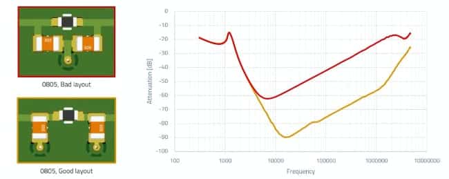
Filter layout examples show the same schematic implemented with different routing and component placement. The “good” layout preserves short loops, compact routing and direct returns, achieving significantly better attenuation—on the order of tens of decibels—than a functionally identical but geometrically poor layout. Conversely, placing filter parts on the board backside and connecting them via elongated via paths to the main transmission line can degrade attenuation by around 10–20 dB in some frequency bands.

For high‑speed interfaces like HDMI, placing AC‑coupling or blocking capacitors on the less optimal side or with long stubs can also compromise eye diagrams and signal integrity, not just EMC. The design message is clear: filter performance is a system property of both the schematic and the layout; careful geometry is as important as component values.
Via count vs. parasitic inductance (qualitative)
| Pad connection style | Example via count | Relative parasitic inductance | Expected effect on EMI filter attenuation |
|---|---|---|---|
| Minimal | 1 | 1.0 (reference) | Baseline; higher residual noise |
| Improved | 3 | ~0.75 of single‑via case | Noticeably better high‑frequency attenuation |
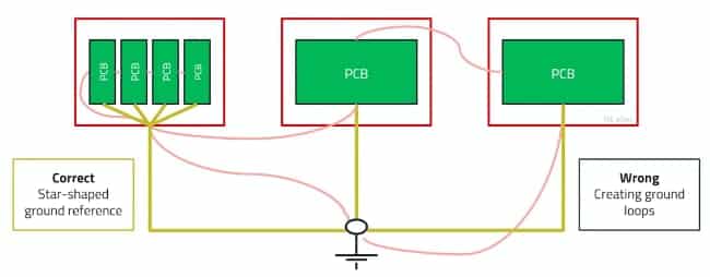
Grounding, star concepts and system‑level interconnects
At system level, how individual PCBs and subassemblies share ground is often decisive. In distributed systems with multiple boards connected by cables, generic expectations that “noise will leave over the cable shield” may not hold due to capacitive and inductive coupling between boards.
Placing all boards on a common low‑impedance reference—typically a solid ground structure—reduces their potential to interfere with each other compared to isolated islands connected only via long harnesses. The area of the conductor has more impact than its thickness due to skin effect: current at high frequency flows near surfaces, so adding area is more effective than thicker copper for lowering high‑frequency impedance.
Star ground concepts work well in low‑frequency power distribution, where the goal is to prevent large current loops in the DC and mains frequency range. At higher frequencies, the dominant reference for a signal becomes the nearest conductive surface, whether that is a ground plane, chassis or shield. In poor stackups, such as a four‑layer board with signal‑signal‑ground ordering, the “ground” reference for the top signal layer may unintentionally be a lower signal layer rather than the ground plane, shaping return paths in undesirable ways.
The webinar also notes that when different departments (mechanical, EMC, electronics, thermal) work independently, later enclosure changes can unexpectedly worsen EMC. For example, adding a highly ventilated housing for thermal reasons can increase openings that compromise shielding, while heatsinks and other metallic structures can create unplanned capacitive or inductive coupling paths.
Heat sinks, gap fillers and EMC
Heatsinks and thermal interface materials are often treated purely as thermal components, but they introduce significant EMC effects. A typical structure of a MOSFET, gap filler, and heatsink forms a capacitor: two metal plates separated by a dielectric. This creates a path for common‑mode currents from fast switching nodes into the heatsink and then into space or nearby structures, increasing radiated emissions.
Gap fillers with higher thermal conductivity tend to incorporate more ceramic particles, raising their effective permittivity and strengthening capacitive coupling. Changing only the gap filler type in a design can therefore shift EMC performance significantly, even if the electrical schematic remains unchanged.
Grounding the heatsink to a well‑defined reference, such as the main ground plane, can dramatically reduce radiated noise. Measurements presented in the webinar show that simply tying a heatsink to ground, even with a straightforward mechanical connection, can lower emissions by roughly 20–30 dB in certain frequency ranges. Designers should thus treat heatsinks and their interface materials as EMC‑relevant components, not just thermal accessories.
Cables, loops and connector placement
Internal cables and harnesses can act as effective antennas if not managed. When engineers assume that short cables “cannot matter,” they often overlook how loop geometry and return paths interact.
Two parallel internal cables forming a loop between boards can behave as a loop antenna, enhancing radiation. Twisting a signal and its corresponding return (or using twisted pairs) reduces loop area and radiated emissions. However, twisting unrelated signal conductors can increase crosstalk, so twisting should be reserved for true forward‑return pairs or differential pairs.
Simple experiments demonstrate that flexible flat cables (FFC) floating between boards exhibit characteristic impedances around typical values such as 125 Ω, but when the cable is attached to a conductive surface with foil at least at one point, its impedance can drop significantly, for example to roughly 60 Ω. From an EMC perspective, mounting a cable close to a conductive surface partly shields it and modifies its antenna behavior. Twisting cables in addition to referencing them to a conductive surface further reduces emissions.
Protective earth (PE) connection placement is another subtle but important factor. A common recommendation is to terminate PE where the cable enters the housing, ensuring a defined reference for shielded cables at the entry point. In modern devices with connectors on multiple sides, implementing this guideline consistently can be challenging, illustrating the limits of generic rules in complex mechanical layouts.
Cable quality itself matters as well. In one example, a shielded USB cable failed EMC tests because its shield was only connected via a short pigtail, effectively creating an antenna at certain frequencies. X‑ray inspection revealed incomplete 360° shield termination. For shielded interfaces like USB and HDMI, engineers should verify shield termination quality, not just rely on cable labeling.
Ferrites, common‑mode chokes and high‑current behavior
Chip ferrites and cable ferrites are ubiquitous EMC mitigation tools, but their selection and application require care. The webinar highlights several aspects:
- Ferrite impedance vs. frequency must be matched to the noise spectrum.
- Real‑world currents during start‑up or transients can be far higher than nominal DC ratings.
- Using a standard chip ferrite in series with reservoir capacitors at the input of a DC‑DC converter can cause very high inrush currents during capacitor charging.
In extreme cases, this inrush can exceed the mechanical strength or thermal limits of the ferrite chip, leading to cracking or open circuits. A failed series ferrite may eliminate both current and EMC issues, but obviously at the cost of functionality.
To tackle this, Würth Elektronik developed a multilayer high‑current pulse ferrite family (MPSB series). Compared with standard chip ferrites, these components include additional conductive paste to improve current handling capability and robustness during high‑current pulses. Datasheets provide maximum current versus pulse length and derating curves for pulse counts over lifetime, allowing designers to verify that the ferrite will survive the expected switching and start‑up events. The trade‑off is that adding conductive material reduces the number of effective windings, lowering the overall impedance; designers must balance desired attenuation with survivability.
For both SMD and cable ferrites, the recommended selection process combines:
- Reserving PCB space early, even with temporary zero‑ohm links, to allow filter retrofits after pre‑compliance testing.
- Using reference designs and example values from IC vendors as starting points where available.
- Performing pre‑compliance EMC measurements and iterating ferrite values and positions.
- Leveraging application notes and filter‑design tools that relate cable length, data rate and desired attenuation to appropriate common‑mode choke or ferrite characteristics.
Standard chip ferrite vs. MPSB pulse ferrite
| Parameter | Standard chip ferrite | MPSB multilayer pulse ferrite |
|---|---|---|
| Intended use | General EMI suppression | EMI suppression with high pulse currents |
| Inrush / pulse robustness | Limited, may crack under surge | Specified pulse‑current ratings |
| Impedance level | Higher for given size | Lower (fewer effective windings) |
| Datasheet guidance | DC current, impedance curves | DC current, impedance + pulse derating curves |
Ground spacers, mechanical hardware and EMC behavior
Mechanical spacers and mounting hardware influence EMC in subtle ways. Purpose‑designed SMD ground spacers with suitable plating and geometry provide low‑impedance, mechanically robust connections between PCB ground and chassis, improving RF grounding performance. Surface treatments such as tin coatings improve solderability and maintain low contact impedance while resisting oxidation.
In contrast, generic zinc‑ or nickel‑plated mechanical spacers and screws, chosen for cost or mechanical reasons, can exhibit high magnetic permeability and frequency‑dependent impedance. In some bands they behave somewhat like ferrites, altering return paths and local fields in unpredictable ways. Since their effect is not broadband or intentionally designed, they may pass certain frequencies and obstruct others, potentially allowing problematic frequency components to find alternative and unintended return paths.
The practical implication is that mechanical choices and plating materials should be coordinated with EMC objectives. Where ground spacers also serve as RF grounding elements, components designed specifically for EMC should be preferred over arbitrary mechanical hardware.
Non‑impedance‑controlled connectors and high‑speed links
Many standard board‑to‑board and wire‑to‑board connectors were not originally designed for high‑speed differential signaling, yet engineers frequently use them for interfaces like USB or similar protocols. To support this, Würth Elektronik measured eye diagrams and bandwidth characteristics for various connector types under USB‑like signaling.
For example, tests on a pin‑header arrangement with a certain pitch show that USB 2.0 and USB 3.2 Gen1 (10 Gbit/s) signals can be transmitted with acceptable eye diagrams up to particular limits, while 20 Gbit/s transmission is marginal or not recommended in that configuration. Increasing the pitch to 2 mm in an otherwise similar connector significantly improves performance, allowing acceptable transmission up to 20 Gbit/s in the tested scenario. This underscores that connector geometry, pitch and internal structure are critical for signal integrity.
Cable handling also plays a role: carefully twisted conductor pairs with controlled geometry produced consistent characteristic impedance and clean eye diagrams in the measurements. In contrast, loosely bundled or randomly oriented conductors showed high, variable impedance and heavily degraded eye openings, sometimes failing even USB 2.0.
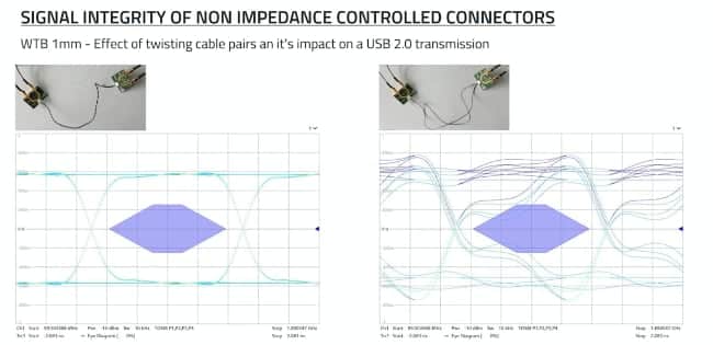
The company offers characterization data for multiple connectors and can test specific protocols, such as HDMI, using the appropriate eye diagram masks when customers provide protocol and compliance requirements. This allows engineers to assess whether a chosen non‑impedance‑controlled connector is suitable for a given high‑speed application or whether a different series is required.
Example: USB over pin header (qualitative)
| Connector pitch | USB 2.0 (480 Mbit/s) | USB 3.2 Gen1 (10 Gbit/s) | USB at 20 Gbit/s |
|---|---|---|---|
| ~1 mm class | Acceptable | Acceptable | Marginal / not recommended |
| 2 mm | Acceptable | Acceptable | Acceptable in tested setup |
Impedance tuning and connector design
Impedance control in connectors is fundamentally governed by the relationship between inductance and capacitance per unit length, often expressed as Z0=LCZ_0 = \sqrt{\frac{L}{C}}. Adjusting internal structures to increase capacitance or reduce inductance can move the connector toward the system’s target impedance, such as 50 Ω or 100 Ω differential. For instance, some modular jacks include internal metal plates that act as capacitive elements, compensating inductive effects and improving overall characteristic impedance. Simulation and 3D field modeling help refine these structures before production.
System designers can further fine‑tune impedance with external capacitors or layout adjustments, but there are limits to what can be corrected after the fact. Reviewing connector characterization data early in the design is therefore important for high‑speed applications.
Design‑in notes for engineers
Based on the webinar content, several practical guidelines emerge for design engineers and purchasing teams working with connectors and passives in EMC‑critical designs:
- Treat rise time as a primary EMC parameter. Selecting interfaces or configurations with unnecessarily fast edges can multiply EMC challenges and constrain layout options.
- Design controlled return paths on every layer. Minimize plane splits and provide intentional high‑frequency return connections between separate ground regions where safety allows.
- Dimension vias and pad connections for low inductance at critical points. Use multiple vias on power and ground pads, especially around filters and decoupling capacitors.
- Plan filter and ferrite locations early. Reserve space and routing options for common‑mode chokes, chip ferrites and RC filters, even if initial prototypes omit them.
- Coordinate thermal and EMC decisions. Evaluate how heatsinks, gap fillers and mechanical supports interact with switching nodes and ground references.
- Verify cable and connector behavior. Request or consult eye diagrams, s‑parameter data and EMC‑related characterization for connectors intended for high‑speed or noisy interfaces.
- Use near‑field scanning and pre‑compliance testing. Visualizing field distributions and measuring partial systems early typically saves one or more design iterations compared to relying solely on final full‑compliance tests.
These notes highlight that EMC is inherently cross‑disciplinary, bridging PCB layout, mechanical design, thermal management, component selection and system architecture.
Considerations for purchasers and component selection
From a component procurement perspective, several points are worth emphasizing:
- Connector selection should consider not just pin count and mechanical form factor, but also documented signal‑integrity behavior at the target data rates.
- Specialized EMC components such as high‑pulse‑current ferrites or ground spacers can avoid field failures and reduce redesign risk, which often outweighs small unit‑price differences.
- Coordinating with suppliers to obtain detailed application notes, test data and modeling files supports more robust design reviews and reduces uncertainty in EMC margins.
Purchasers can add value by ensuring that the chosen component series have the necessary documentation and characterization for the intended EMC use case.
Technical highlights
The following technical points from the webinar are particularly relevant when working with passive components, connectors and EMC:
- Fast edges increase required bandwidth and EMC stress; reducing edge speed where protocol allows is a powerful mitigation.
- Return paths are as important as forward traces; interruptions in reference planes generate radiating loops and crosstalk.
- Plane area beats thickness for high‑frequency ground impedance due to skin effect.
- Multiple vias in parallel at critical connections significantly reduce parasitic inductance and improve filter performance.
- Layout changes alone, without altering a filter schematic, can yield tens of decibels difference in attenuation.
- Heatsinks and gap fillers form capacitors to switching nodes, and their connection or isolation strongly influences common‑mode emissions.
- Twisted pairs and cable routing relative to conductive surfaces have a measurable impact on characteristic impedance and radiation.
- Non‑impedance‑controlled connectors can sometimes support high‑speed protocols if characterized, but performance depends strongly on geometry and pitch.
- High‑current‑pulse ferrite series with defined pulse ratings can prevent ferrite damage in power applications while still providing useful attenuation.
These points offer a concise checklist for reviewing designs from an EMC perspective before committing to hardware.
Example: USB over non‑impedance‑controlled connectors
A practical scenario discussed is transmitting USB signals over standard wire‑to‑board or pin‑header connectors. Engineers often do this for convenience, but need to check:
- Whether USB 2.0, 3.x Gen1 or higher rates are intended.
- Whether the connector series has measured eye diagrams and bandwidth data for the desired rate.
- How cable orientation, twisting and routing near ground affect characteristic impedance and eye quality.
The webinar’s measurements show that some standard connectors can support up to 10 Gbit/s or even 20 Gbit/s in specific configurations, while others are unsuitable even for 480 Mbit/s when used with uncontrolled cabling. This underscores the importance of using available characterization data instead of assuming any connector can carry any protocol.
Conclusion
Key takeaways for EMC‑aware connector and PCB design
By the end of this material, the reader should recognize that EMC performance is determined by a combination of signal edge characteristics, return‑path control, parasitic management and judicious use of connectors and passive components. Good EMC outcomes come from deliberate layout choices—such as solid reference planes, minimized loops, appropriate via usage and controlled cable routing—rather than last‑minute shielding fixes.
Design engineers can apply these principles to reduce the number of EMC test iterations: reserving space for filters and ferrites, grounding heatsinks intelligently, choosing connectors with known signal‑integrity performance and coordinating mechanical and thermal decisions with EMC needs. As a next step, readers may wish to explore Würth Elektronik’s application notes, near‑field scanning examples and component family documentation to translate these concepts into concrete design rules and part choices for their own systems.
FAQs
Because EMC behavior is dominated by edge speeds, return paths and parasitics defined in the PCB design. Once the layout and connector concept are fixed, test‑chamber fixes can only add band‑aids like shields and ferrites rather than solving the root cause.
Shorter rise and fall times increase the harmonic content of a signal and turn every trace into a transmission line at lower lengths. This makes radiation, crosstalk and impedance mismatches more likely, especially on high‑speed interfaces like USB and HDMI.
Always route signals with a continuous, low‑impedance return path on an adjacent reference plane. Avoid split planes, slots and long detours that force return currents to form large loops, because those loops act as antennas.
Use multiple vias in parallel for decoupling capacitors, common‑mode chokes and connector grounds. This lowers parasitic inductance and can improve filter attenuation by several tens of decibels compared with single‑via connections.
A heatsink and power device form a capacitor through the gap filler, creating a path for common‑mode currents into the heatsink and chassis. The choice of gap‑filler material and whether the heatsink is bonded to ground can significantly change radiated emissions.
Check not only the nominal impedance and DC current rating, but also pulse‑current capability and derating curves. Standard chip ferrites can crack under inrush pulses, so high‑pulse‑current parts such as multilayer pulse ferrites are better suited for DC‑DC inputs.
Yes, in some cases, but only if the connector series has characterization data such as eye diagrams and bandwidth measurements at the target data rate. Geometry, pitch and cable handling strongly influence whether a given connector can support, for example, USB 3.x reliably.
Twisting true signal‑return or differential pairs, and routing them close to conductive reference surfaces, reduces loop area and radiation. Randomly bundling or twisting unrelated conductors can increase crosstalk and degrade eye diagrams.
They should ensure that components come with documented signal‑integrity and EMC behavior, including application notes, test data and models, and prioritize parts designed for high‑speed and high‑pulse environments over cheaper generic options.
Near‑field scanning and partial‑system pre‑compliance tests reveal hot spots and coupling problems early, helping teams adjust layout, component placement and grounding before committing to expensive final compliance tests.
How to design EMC‑compliant PCB layouts and connectors
- Step 1: Define interface speeds and edge‑rate limits
Start by listing all high‑speed interfaces (for example USB, HDMI, LVDS) and their required data rates. Where the protocol allows, select device configurations or drivers with controlled or slower edge rates to avoid unnecessary EMC stress.
- Step 2: Plan stackup and reference planes
Choose a layer stack where every high‑speed signal layer is adjacent to a solid reference plane. Avoid signal‑signal‑ground sequences for critical nets, and ensure that return currents can flow directly under or beside their forward traces.
- Step 3: Route with continuous return paths
During layout, avoid slots, splits and long cut‑outs in ground or power planes under high‑speed traces. When unavoidable, add controlled high‑frequency return paths, such as capacitors between reference regions, within safety limits.
- Step 4: Minimize loop areas in critical paths
Identify high‑di/dt loops around converters, filters and connectors, and place components to keep these loops compact. Shorten trace lengths and ensure that the forward and return paths run close together to reduce magnetic‑field radiation.
- Dimension vias and pads for low inductance
Use multiple vias for power, ground and filter components, especially for decoupling capacitors and common‑mode chokes. Avoid thin thermal spokes on EMC‑critical connections, as they increase parasitic inductance and degrade filter performance.
- Step 6: Treat heatsinks and gap fillers as EMC components
When adding heatsinks and thermal interface materials, model or at least qualitatively assess the capacitance they introduce from switching nodes to the heatsink. Decide whether the heatsink should be tied to ground and select gap fillers with suitable dielectric properties.
- Step 7: Select ferrites and chokes with pulse ratings
For input filters and high‑current paths, choose ferrites and chokes with specified pulse‑current capability and derating data. Verify that these parts can withstand inrush and transient events over the product lifetime.
- Step 8: Choose and characterize connectors for high‑speed links
For non‑impedance‑controlled connectors, obtain vendor eye diagrams or S‑parameter data at the intended data rate. Combine these with controlled cable geometries and, where possible, twisted pairs to keep characteristic impedance within acceptable limits.
- Step 9: Design cable routing and grounding
Route internal cables close to reference surfaces and keep forward‑return pairs together. Terminate protective earth and cable shields near the enclosure entry, ensuring short, low‑inductance paths for shield currents.
- Step 10: Perform pre‑compliance EMC measurements
Use near‑field scans and partial‑system EMC tests to validate that layout, connectors and filters behave as intended. Iterate placement, via usage and grounding based on measurement results before finalizing the design.
Source
This article is based on the Würth Elektronik webinar “EMC with EMC – EMC‑compliant design with electromechanical connectors” and its transcript, with additional editorial structuring and commentary for design engineers and component purchasers.
References

