The move toward 800 V DC power architectures is forcing EMC filter design to become more rigorous, not just in component voltage rating, but in how common-mode and differential-mode noise are separated, modeled and verified.
Based on the Würth Elektronik webinar, this article explains a practical design guide for engineers working on high-voltage DC power converters, filters and related subsystems.
The example hardware is an isolated flyback converter used as a safe noise source rather than a live 800 V system, but the filter design method remains valid for real 800 V DC applications as long as component voltage class, creepage and clearance are chosen correctly. The useful takeaway is that EMC performance depends as much on the structure of the filter and the measurement setup as on nominal component values.
Key features and benefits
The article and webinar video provides a structured method for designing an 800 V DC EMC filter from measured attenuation targets back to practical X capacitors, Y capacitors, common-mode choke values and layout rules. That is valuable because high-voltage filters are often over-designed when engineers do not first separate common-mode and differential-mode noise.
For design teams, the practical benefits are clear:
- Separate common-mode and differential-mode noise before sizing the filter.
- Use realistic LISN impedance values in calculation and simulation.
- Select voltage-rated parts that also satisfy surge, creepage and clearance requirements.
- Validate the result on a bench setup that mimics the EMC chamber as closely as possible.
Noise mechanisms in 800 V DC filters
Differential-mode noise flows between the positive and negative DC rails along the intended circuit path, so it is usually easier to trace in the schematic and easier to address with LC, π\pi, or T-type filters placed between the rails. As demonstrated, differential-mode noise is linked mainly to high current slew rate and ringing caused by parasitic inductance, including component ESL and layout inductance.
Common-mode noise is harder to control because it returns through parasitic capacitances and protective-earth paths that are usually not explicit in the schematic. The webinar explains that common-mode interference is primarily driven by high dv/dt\mathrm{d}v/\mathrm{d}t, and is therefore addressed with common-mode chokes, Y capacitors and careful shielding or chassis coupling.
Filter building blocks at a glance
| Element | Main role | Noise mode affected | Practical note |
|---|---|---|---|
| MOV / varistor | Clamps surge events ahead of the filter | Indirectly both | The example uses a 20 mm MOV to handle surge energy and reduce stress on downstream parts. |
| X capacitor | Shunts noise between DC+ and DC− | Mainly differential mode | In 800 V DC systems, surge capability matters as much as nominal capacitance. |
| Common-mode choke | Adds series impedance in both lines together | Mainly common mode | Leakage inductance also helps differential-mode attenuation. |
| Rod-core inductor | Adds extra series impedance at higher frequency | Differential mode and HF CM support | Useful when the filter needs better attenuation above the main conducted band. |
| Y capacitor | Returns common-mode current to PE / chassis | Common mode | DC systems can often use higher Y-capacitance values because 50/60 Hz leakage current is not the same limitation as in AC mains filters. |
| Low-ESL PE connection | Reduces parasitic inductance in the earth return path | Common mode | The webinar strongly favors direct low-inductance chassis coupling for Y capacitors. |
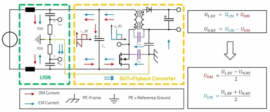
Why the LISN matters
Line impedance stabilization network (LISN) plays significant role in filter design as it depends on the impedance seen during measurement. For differential-mode analysis, the current flows through two 50 Ω resistors in series, so the effective LISN impedance is 100 Ω, while for common-mode analysis the relevant 50 Ω paths appear in parallel to earth, giving 25 Ω.
That distinction is critical because using only the combined measured spectrum tends to force unnecessary filter margin. The recommendation therefore is to measurie both LISN outputs simultaneously and using oscilloscope math to derive differential mode with (CH1−CH2)/2(\text{CH1} – \text{CH2})/2(CH1−CH2)/2 and common mode with (CH1+CH2)/2(\text{CH1} + \text{CH2})/2(CH1+CH2)/2, which avoids the common mistake of designing both sections for the same attenuation target.
Separate treatment of common-mode and differential-mode noise
| Item | Differential mode | Common mode |
|---|---|---|
| LISN impedance used in design/simulation | 100 Ω | 25 Ω |
| Source model | Low-impedance voltage source | High-impedance current source |
| Main filter structure | CLC / π\piπ filter | LC filter |
| Typical attenuation slope | 60 dB/decade | 40 dB/decade |
| Main components | X capacitors, leakage inductance, rod-core inductors | CM choke, Y capacitors, PE return path |
| Oscilloscope math | (CH1−CH2)/2(\text{CH1} – \text{CH2})/2(CH1−CH2)/2 | (CH1+CH2)/2(\text{CH1} + \text{CH2})/2(CH1+CH2)/2 |
Minimum filter structure
A practical 800 V DC filter design starts at the source or LISN side with surge protection, then includes X capacitors, a common-mode choke, optional rod-core inductors and Y capacitors to protective earth near the device under test. A second X capacitor on the DUT side is optional but beneficial because it turns the differential-mode path into a CLC, or π\pi, filter with a steeper attenuation slope.
The ordering of the parts is not arbitrary. For common-mode filtering, Y capacitors belong close to the DUT because they create a lower-impedance return path for noise currents back to their source, while for differential-mode filtering the leakage inductance and series inductors should sit next to the low-impedance noise source and work against the higher LISN-side impedance.
Safety and spacing requirements
There is no single dedicated standard focused only on 800 V DC data-center filters, but the required safety framework still comes from existing standards that define overvoltage category, surge test level, creepage, clearance and insulation class. In practice, these systems as typically OVC II or OVC III, which implies surge tests in roughly the 4 kV to 6 kV range, considerably above what many low-voltage AC designs are built for.
Clearance values are roughly 5.5 mm to 8 mm for basic insulation, while creepage can range from around 2.4 mm up to 16 mm depending on pollution degree and CTI. Reinforced insulation effectively pushes those spacing requirements much higher, which means component package pitch and PCB geometry must be reviewed together rather than separately.
Technical highlights
The following table presents several concrete part-selection rules that are especially useful for engineers and sourcing teams. Between the DC rails, the preferred solution is an X1 capacitor because it can typically withstand up to 5 kV surge, while X2 capacitors usually need to be used in series if the design must satisfy a 4 kV-class surge requirement.
For Y capacitors to protective earth, the Y2 parts as a more practical choice than Y1 in many 800 V DC filters because Y2 can offer sufficient surge and working-voltage performance with lower cost and size. The common-mode choke should be at least in the 1 kV voltage class and should provide suitable creepage and clearance directly at the component level.
Example component selection logic for 800 V DC filters
| Component type | Webinar guidance | Why it matters in practice |
|---|---|---|
| X capacitor between DC+ and DC− | Prefer X1 where available; if X2 is used, series connection may be needed | Working voltage alone does not guarantee surge robustness. |
| Y capacitor to PE | Y2 may be sufficient for many 800 V DC systems | Often the best trade-off between size, cost and required voltage capability. |
| Common-mode choke | Use an HV-rated choke with adequate creepage and clearance | The choke must satisfy both EMC and insulation needs. |
| MOV | Use a 20 mm part with sufficient energy handling | A small varistor may not absorb enough surge energy. |
| Terminal block | Select for voltage, current, creepage and clearance together | Mechanical interface choices can limit the whole design. |
The specific component in the examples include a WE-CMBHV common-mode choke rated up to about 1.25 kV DC and up to roughly 22 A, a 20 mm varistor with about 360 pF parasitic capacitance, Y2 capacitors from 1 nF to 470 nF with up to about 1000 V DC capability, and FTXH film capacitors as a possible X2 option when series use is acceptable. For the demonstration hardware, a DC-link capacitor was used in the X-capacitor position because a dedicated X1 option was not yet available, but the speaker clearly notes that this is a demo compromise rather than a universal replacement for an X1 safety capacitor.
Example design targets from the example
| Parameter | Value used in the example | Comment |
|---|---|---|
| Switching frequency of interest | 300 kHz | Dominant low-frequency emission peak in the example setup |
| Required common-mode attenuation | About 60 dB at 300 kHz | Derived from separated measurement |
| Required differential-mode attenuation | About 40 dB at 300 kHz | Lower target avoids DM overdesign |
| Common-mode corner frequency | About 9.5 kHz | Based on LC filter slope and target attenuation |
| Differential-mode corner frequency | About 65 kHz | Based on CLC filter slope and target attenuation |
| Required common-mode inductance | About 1.5 mH | Practical selection should include tolerance margin |
| Example total differential-mode inductance | About 35 µH | Includes leakage inductance plus rod-core inductors |
| Effective X-capacitance target | About 170 nF | Because the two X capacitors act in series at RF |
Calculation flow
The design method starts by identifying the lowest significant emission frequency, which in the example is the converter switching frequency at about 300 kHz. Because lower corner frequencies require larger magnetics and capacitance, we intentionally size the filter around this low-frequency dominant peak rather than around higher-frequency harmonics.
For common mode, the target attenuation is about 60 dB at 300 kHz, and for differential mode it is about 40 dB. Using the respective filter slopes, the example derives corner frequencies of about 9.5 kHz for the common-mode LC section and about 65 kHz for the differential-mode CLC section.
For the common-mode branch, the proposed starting point is the Y-capacitance, because DC operation removes the usual mains-frequency leakage-current limitation that constrains Y-capacitor size in AC filters. We setup four 47 nF Y capacitors and then derive a required common-mode inductance of about 1.5 mH, while also recommending more nominal inductance in practice because common-mode chokes can have around ±30% tolerance and additional temperature drift.
For the differential-mode branch, the leakage inductance of the common-mode choke is extracted from the impedance curve rather than taken from a directly stated datasheet number. In the example, a 9.6 Ω differential-mode impedance at 100 kHz corresponds to about 15 µH leakage inductance, and with the two rod-core inductors added, the total differential-mode inductance reaches about 35 µH.
The effective X capacitance is then calculated from the series combination of the two X capacitors used in the π\pi structure. With the chosen differential-mode corner frequency and total series inductance, the required effective capacitance is about 170 nF, which leads to individual X-capacitor values on the order of roughly 330 nF to 400 nF each when identical capacitors are used.
Typical applications
Although the webinar example uses a flyback converter as a noise source, the design method is relevant to a wider range of 800 V DC systems. The speaker explicitly frames the topic in the context of growing 800 V power networks and data-center applications, but the same workflow is also relevant to industrial DC links, EV charging hardware, onboard power converters and other high-voltage DC subsystems.
In all of these applications, the same practical question appears: how much common-mode attenuation and how much differential-mode attenuation are really needed at the dominant emission frequency. Once that is known, the filter can be sized with much more confidence and less unnecessary bulk.
LTspice simulation strategy
The example uses LTspice to check insertion loss before hardware validation. For differential mode, the model includes the 100 Ω LISN impedance, the MOV capacitance, X capacitors, rod-core inductors, the common-mode choke and a low-impedance source representing the converter input, while for common mode the model uses 25 Ω LISN impedance, Y capacitors to ground and a high-impedance current source with optional series resistance to represent the DUT.
The reported simulation result is a good match to the analytical target. Around 300 kHz, the differential-mode insertion loss comes out at about 40 dB to 42 dB and the common-mode insertion loss at about 62 dB, with both remaining stable up to roughly 10 MHz before declining at higher frequency.
Bench measurement and verification
The webinar places unusual emphasis on building a realistic bench setup, which is one of its strongest practical sections. The recommended arrangement includes an FFT-capable oscilloscope with logarithmic frequency display and 9 kHz resolution bandwidth, an isolation transformer, a LISN, the filter PCB, the noise source, the load and a conductive metal plate acting as an EMC-chamber reference plane.
That metal reference plane matters because common-mode currents need a defined return path to produce repeatable results. The case study example also uses steel spacers and conductive mesh to ensure a low-impedance connection from the Y capacitors and LISN earth connection to the metal plate, minimizing variation due to contact quality.
With no filter installed, the example system produces strong emissions at 300 kHz. After the designed filter is added, the measured combined spectrum stays comfortably below the target limit from about 300 kHz to around 10 MHz, but the margin becomes narrow in the 15 MHz to 25 MHz region because the through-hole Y capacitors have too much ESL for high-frequency common-mode suppression.
Through-hole and SMD Y capacitors in the same filter
| Approach | Strength | Limitation | Best use |
|---|---|---|---|
| Through-hole Y capacitors | Higher capacitance, strong low-frequency common-mode attenuation | Higher ESL reduces high-frequency performance | Main filtering below about 10 MHz |
| Small SMD Y capacitors in series pairs | Lower ESL, better high-frequency bypass behavior | Lower capacitance and stricter HV spacing constraints | Improving 10 MHz to 30 MHz margin |
| Hybrid approach | Broad-band common-mode performance | Slightly more complex layout | Best overall compromise in compact filters |
To fix the high-frequency weakness, we add small low-ESL SMD Y capacitors in parallel with the existing through-hole Y capacitors. Because spacing still matters at 800 V, the SMD parts are used in series pairs, and the result is more than 10 dB additional insertion loss improvement at the upper end of the conducted band.
Design-in notes for engineers
The layout guidance is practical and worth preserving almost verbatim in design reviews. Creepage and clearance between positive and negative rails must match the chosen insulation class, inductors and capacitors should be oriented at roughly 90° to each other to reduce magnetic and electric coupling, and protective-earth routing for Y capacitors should be short, wide and connected directly to shielding or chassis rather than meandered through the PCB.
The Y-capacitor earth returns should not be implemented as ordinary PCB routing under the filter, because that can increase inductance and even convert common-mode noise into differential-mode behavior. The cutouts used to improve creepage are generally acceptable and that large copper polygons under the filter should be avoided for both safety and field-coupling reasons.
Temperature and tolerance also deserve margin. Inductors can lose roughly 20% to 40% of inductance at low temperature in worst cases, while capacitors can lose about 5%, and common-mode chokes may already carry ±30% production tolerance, so a design that only just meets the target on paper is unlikely to remain robust across operating conditions.
Other practical Q&A points are also useful in real programs:
- Bleeder resistors are generally not required for Y capacitors in fixed DC systems.
- Damping networks are not mandatory in most filters, but may be needed if surge excitation coincides with a strong LC resonance.
- In automotive 800 V systems with additional superimposed test voltages, standard X1 or X2 capacitors may not be sufficient, and higher DC working-voltage parts may be required.
- Earth leakage current through Y capacitors is not the same issue in DC as it is in 50/60 Hz AC systems, which is one reason larger Y-capacitance values are attractive here.
Conclusion and Take Away
The key lesson presented herein is that 800 V DC EMC filters should not be designed as generic high-voltage versions of low-voltage mains filters. The right method is to separate common-mode and differential-mode emissions first, derive the required attenuation for each path, and then calculate, simulate and verify the filter as two related but distinct problems.
For engineers, that means better use of X capacitors, Y capacitors, common-mode chokes and auxiliary rod-core inductors, plus better control of chassis return paths and layout parasitics. For purchasing teams, it means that surge capability, creepage, clearance and real high-frequency behavior are often more important than the headline capacitance or inductance value alone.
Next steps
A practical next step after reading this article is to repeat the webinar workflow on your own converter: measure the combined spectrum, separate common-mode and differential-mode noise, derive attenuation targets at the dominant low-frequency peak, and then validate the selected topology in LTspice before committing to hardware spins. Where exact values remain application-dependent, the final selection should be confirmed against the manufacturer datasheet and the relevant insulation and EMC standards for the target installation class.
Source
This article is based on Würth Elektronik webinar, adapted into a technical summary for engineers working with high-voltage EMC filters and related passive components.
References
- Würth Elektronik webinar: Calculation, Simulation and Measurement of 800V EMC Filters
- Application note ANP015 – Single-phase EMC filters
- Würth Elektronik interference suppression capacitors
- WE-CMBHV high-voltage common-mode chokes
- Würth Elektronik SMD spacer overview

