

Electromagnetic interference (EMI) remains one of the key challenges in modern electronics, affecting both signal integrity and the reliable operation of power and data systems. In low‑voltage and mains applications, varistors and common mode chokes are two of the most important passive components for overvoltage protection and EMC filtering, yet they are also frequently misunderstood and mis‑applied.
This article distills the main engineering insights from a Würth Elektronik technical webinar on EMC design fundamentals, focusing on how to select and use varistors and common mode chokes safely and effectively in real‑world designs.
Key features and benefits
Varistors and common mode chokes work together within typical mains and low‑voltage EMC filters to limit surge and ESD stress and to suppress common‑mode noise without degrading the desired power or data signal. A typical single‑phase mains filter will contain a fuse holder, varistor, discharge resistor, common mode choke, and X/Y capacitors, with each component contributing a distinct protection or filtering function.
Varistors (both through‑hole disc types and multilayer SMD types) provide fast, non‑linear clamping of overvoltage events, diverting surge energy away from sensitive circuitry once the voltage exceeds their breakdown region. Common mode chokes, built from at least two windings on a shared ferrite or nanocrystalline core, present high impedance to common‑mode currents while leaving differential‑mode currents largely unaffected, helping designs pass CISPR/IEC EMI limits without compromising power or signal integrity.

Key Takeaways
- Surge, EFT and ESD are distinct overvoltage phenomena with different energy and repetition profiles, so they require different protection strategies and component ratings.
- THT disc varistors offer high surge energy handling and wide voltage range for mains and DC, while multilayer SMD varistors are better suited to compact, lower‑energy ESD and transient protection on data and low‑power lines.
- TVS diodes and multilayer varistors differ mainly in clamping behaviour and capacitance; low‑capacitance ESD devices are essential for preserving signal integrity on high‑speed interfaces such as USB and Ethernet.
- Common mode chokes present high impedance to common‑mode noise but low impedance to differential‑mode signals, allowing efficient EMC filtering without saturating under normal load current.
- Winding style (bifilar vs sectional), core material (MnZn, NiZn, nanocrystalline) and parasitic elements strongly influence the attenuation vs frequency profile, so engineers should select chokes based on impedance curves rather than inductance alone.
- For mains filters, sectional‑wound chokes and appropriate creepage and clearance distances are required to meet IEC safety standards, while leakage inductance can be exploited to attenuate high‑frequency differential‑mode noise without affecting 50/60 Hz.
- Proper placement of varistors, TVS diodes and common mode chokes—especially near connectors and system boundaries—significantly improves EMC performance and reduces the risk of long‑term component ageing or premature failure.
Surge and transient environment overview
International EMC standards define different overvoltage phenomena that protection components must withstand and mitigate:
- Surge (IEC 61000‑4‑5) is typically associated with lightning and large switching events, characterized by high voltage, high current, low frequency, and high energy per pulse.
- Electrical Fast Transient/Burst (EFT/B, IEC 61000‑4‑4) arises from industrial events such as switching of inductive loads, with high voltage, low current, low energy per pulse but very high repetition.
- Electrostatic discharge (ESD, IEC 61000‑4‑2) originates from contact or air discharges between bodies, with very high voltage, relatively low current, low energy, and low repetition rate.
From an energy perspective, ESD has the highest voltage but significantly lower energy than surge and EFT, while EFT bursts can reach energy levels around one joule when many pulses are combined into a burst. This difference in waveform characteristics is central to selecting appropriate protection components and understanding their stress profiles over lifetime.
| Overvoltage | Voltage | Current | Rise time | Pulse length | Energy |
|---|---|---|---|---|---|
| Surge | 0.5–4 kV | 0.1–2 kA @ 2 Ω load | 1.25 µs | 50 µs | 10–80 J |
| EFTB | 0.5–4 kV | 10–100 A @ 50 Ω load | 5 ns | 15 ms | 100–1000 mJ |
| ESD | 4–15 kV | 1–50 A @ 50 Ω load | 0.8 ns | 60 ns | 1–10 mJ |
Typical applications
Varistors and common mode chokes appear in a wide range of applications, from AC mains filters to low‑voltage DC power and high‑speed data interfaces.
- Single‑phase AC mains filters for SMPS, motor drives, and industrial equipment use THT varistors with sectional‑wound common mode chokes and X/Y safety capacitors to meet IEC creepage/clearance requirements and pass conducted EMI tests.
- DC power lines in LED matrices, power supplies, and CAN nodes benefit from DC‑rated common mode chokes chosen for their current rating and impedance profile, often placed close to connectors to block conducted noise at system boundaries.
- High‑speed data lines such as USB and Ethernet incorporate dedicated common mode chokes (often bifilar wound) with low differential‑mode impedance at the signal frequency and high common‑mode impedance at noise frequencies, plus low‑capacitance ESD TVS diodes or multilayer varistors.
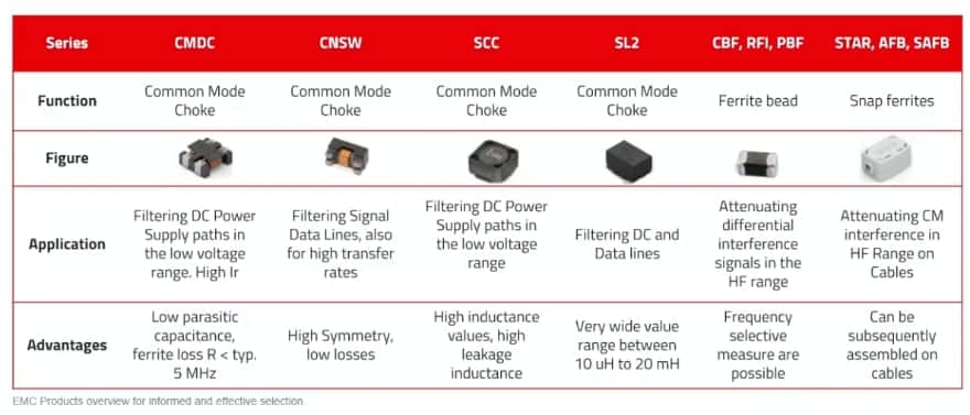
- Mixed interfaces carrying both data and DC power—such as certain communication buses or LED drivers—may use common mode chokes that simultaneously provide differential‑ and common‑mode attenuation at specific frequency bands, as demonstrated by Würth Elektronik’s SL5 series.
In all of these use cases, proper placement of protection and filter elements—especially locating the common mode choke close to the connector—helps prevent noise from propagating into or out of the PCB, improving both EMC performance and system robustness.
| Applications | Probable Noise Source | Main Frequency (reference) | CMC benefit |
|---|---|---|---|
| Power supplies, IoT, LED drivers | Active Switching | 100 kHz – 1 MHz | Blocks CM Noise along cables |
| Cameras, robotics, PoE | Inrush / Capacitive Load | < 1 kHz | Dampens overshoot and ringing |
| Instrumentation | Ground loop or floating reference | 500 kHz – 50 MHz | Suppresses CM |
| Power + Data | Fast buses: USB, WiFi, CAN | 10 MHz – 500 MHz | Reduces Common mode coupling of digital signals on DC line |
| Industrial | EMI from Motors/ Relays | 10 kHz – 5 MHz | Isolates DC line from inductive noise sources |
Technical highlights
Varistor structure and behaviour
A classic disc varistor consists of three main layers: an outer epoxy insulation, internal silver or copper electrodes, and a zinc oxide ceramic core formed from many grains. At the microscopic level, the grains act as conductive regions and the grain boundaries act as barriers to current flow. When the applied voltage is low, only leakage current flows through the device; once the voltage across the electrodes becomes sufficiently high, the barriers break down and current can flow across many grain boundaries, rapidly increasing current in the clamping region.
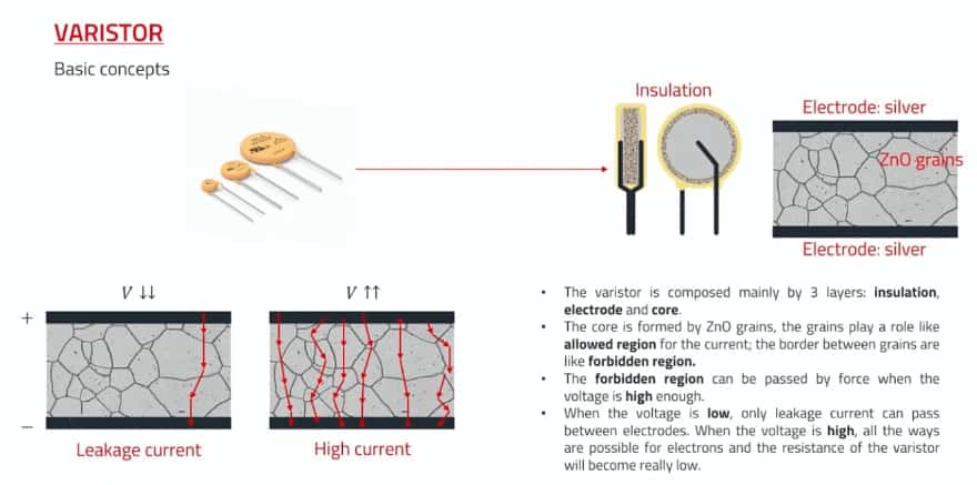
The I–V characteristic of a THT varistor can be divided into four regions:
- Leakage region: current below 0.1 mA for 5 mm discs and below 1 mA for larger devices; the voltage at this current is the breakdown voltage.
- Working voltage region: defined as a voltage at least about 25% higher than the circuit’s normal operating voltage, ensuring the varistor does not conduct significantly during normal operation.
- Operating (clamping) region: between breakdown and the maximum rated surge current, where the varistor is considered “active” and clamps overvoltage pulses to protect the load.
- Destruction region: beyond the maximum surge current, where the device is close to failure and the curve is no longer guaranteed.
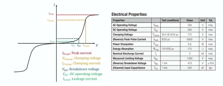
Multilayer varistors (MLV) share the same zinc‑oxide grain conduction mechanism but use multiple interdigitated silver electrodes in an SMD stack, giving a much smaller package size.
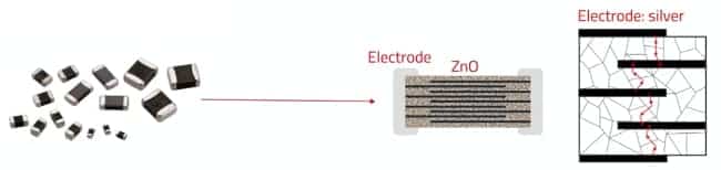
Compared to THT discs, multilayer types have lower working voltage range, lower maximum surge current and energy capability, but faster response time and significantly lower capacitance—important in data‑line ESD protection.
TVS diodes and snapback effects
TVS diodes provide an alternative surge and ESD protection technology based on silicon p–np\text{-}np-n junctions. A typical device comprises a semiconductor chip, protective plastic package, and copper leads connected to the junction.
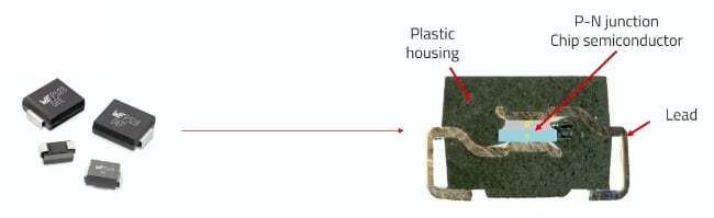
In unidirectional TVS diodes, forward conduction starts once the forward voltage exceeds about 0.6–0.7 V, while in reverse direction the diode remains in leakage up to its working voltage and then transitions into breakdown when the reverse voltage reaches a specified threshold. From breakdown up to the maximum rated current, the diode clamps voltage while allowing substantial current flow.
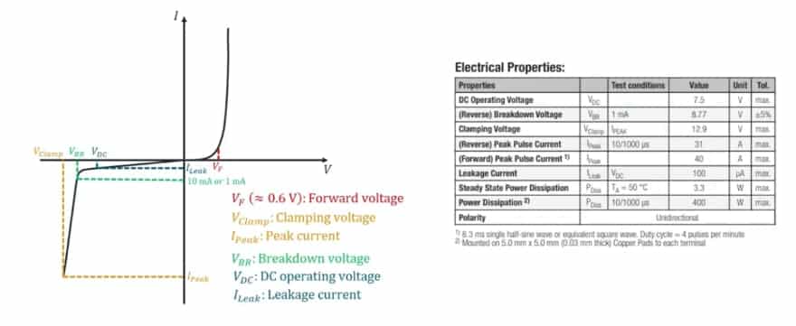
Some TVS diodes exhibit a snapback effect: the device requires an additional voltage above nominal breakdown to trigger a parasitic transistor formed in the package and PCB environment, after which the clamping voltage drops and follows a curve with lower voltage at a given current than a standard diode. This behaviour yields better protection (lower clamping voltage at equal current), at the cost of requiring an extra activation voltage that is generally negligible relative to typical transient pulse amplitudes.
| Serie | THT varistor | Multilayer varistor | TVS Diode |
|---|---|---|---|
| Mount | THT | SMD | SMD |
| VDCV_{DC}VDC (V) | 18–1470 | 3.3–85 | 5–440 |
| IpeakI_{\text{peak}}Ipeak (A) | 100–10000 | 10–200 | 0.6–326.1 |
| WmaxW_{\text{max}}Wmax (J) | 0.7–620 | 0.02–1.10 | – |
| C (pF) | 35–12100 | 70–3600 | 1–20000 |
| Reaction time | <25 ns | <1 ns | <1 ns |
ESD protection and capacitance vs insertion loss
In the ESD protection domain, manufacturers offer multiple families of TVS diodes and multilayer varistors, grouped into standard, high‑speed, and super‑speed areas. The primary differentiator among these families is capacitance: standard types have the highest capacitance, high‑speed intermediate, and super‑speed the lowest. Lower capacitance is critical for high‑speed data‑line applications because it directly affects insertion loss and resonance behaviour.
Insertion loss depends predominantly on impedance, which in turn depends on resistance, inductance, and capacitance of the component. For these low‑inductance ESD devices, resistance remains almost constant with frequency and inductance is negligible, so capacitance dominates.
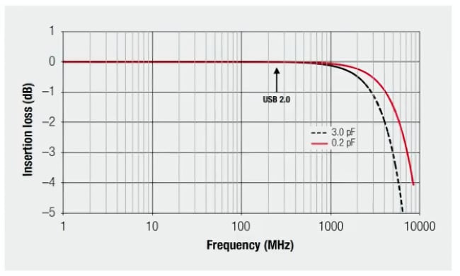
Higher capacitance lowers the resonance frequency and increases insertion loss from that point upward, potentially causing data errors. Design examples provided in the webinar relate typical data‑line frequencies (such as USB or Ethernet bands) to recommended capacitance ranges for ESD suppressors, helping designers choose appropriate low‑capacitance parts for their interface class.
| Component | Surge | EFT/Burst | ESD | Reaction time | Capacitance |
|---|---|---|---|---|---|
| GDT – Gas discharge tube | X | µs | 1 pF | ||
| MOV – Metal Oxide Varistor | X | >25 ns | 10 p–10 nF | ||
| MLV – Multilayer Varistor | X | X | <1 ns | 70 p–14 nF | |
| TVS Diode – Transient Voltage Suppression | X | <1 ns | 0.1–30 pF | ||
| TVSP Diode – TVS Power | X | X | X | <1 ns | 20–2000 pF |
| ESD Suppressor | X | <1 ns | 0.2–100 pF |
| Data line | Data rate | Frequency | Rec. capacitance for ESD device |
|---|---|---|---|
| RS 232 | 115.2 kbit/s | 57.6 kHz | <56 pF |
| 100 kbit/s | 50 kHz | ||
| I²C | 400 kbit/s | 200 kHz | <56 pF |
| 1 Mbit/s | 500 kHz | ||
| RS 422 | 3.4 Mbit/s | 1.7 MHz | |
| 5 Mbit/s | 5 MHz | <10 pF | |
| RS 485 | 12 Mbit/s | 6 MHz | <22 pF |
| CAN | 500 kbit/s | 6 MHz | |
| USB 1.1 | 12 Mbit/s | 6 MHz | <10 pF |
| USB 2.0 | 480 Mbit/s | 240 MHz | <2 pF |
| USB 3.2 Gen 1×1 | 5 Gbit/s | 2.5 GHz | <0.5 pF |
| USB 3.2 Gen 2×1 | 10 Gbit/s | 5 GHz | <0.35 pF |
| USB 3.2 Gen 2×2 | 20 Gbit/s | ||
| USB 4 Gen 2 | 20 Gbit/s | <0.2 pF | |
| USB 4 Gen 3 | 40 Gbit/s | ||
| SATA 1.0 | 1.5 Gbit/s | 750 MHz | <1 pF |
| SATA 2.0 | 3 Gbit/s | 1.5 MHz | <1 pF |
| SATA 3.0 | 6 Gbit/s | 3 GHz | <0.6 pF |
| Ethernet IEEE 802.3u 100BASE-TX | 100 Mbit/s | 125 MHz digital CLK | <6 pF |
| Ethernet IEEE 802.3ab 1000BASE-T | 1 Gbit/s | 31.25 MHz UTP | <3 pF |
| Ethernet IEEE 802.3az 10GBASE-T | 10 Gbit/s | 417 MHz | <2 pF |
| LVDS | 1.325 Gbit/s | <2 pF | |
| HDMI 1.3 | 8.16 Gbit/s | 3.2 GHz (165 MHz) | <0.5 pF |
| HDMI 1.4 | 8.16 Gbit/s | 810 MHz (160 MHz) | <0.5 pF |
| HDMI 2.0 | 14.4 Gbit/s | 6 GHz (600 MHz) | <0.3 pF |
| HDMI 2.1 | 42.6 Gbit/s | 12.8 GHz (600 MHz) | <0.25 pF |
| DisplayPort 1.1 | 8.64 Gbit/s | 1.35 GHz (270 MHz) | <0.6 pF |
| DisplayPort 1.2 | 17.28 Gbit/s | 2.7 GHz (270 MHz) | <0.6 pF |
| DisplayPort 1.3 | 25.92 Gbit/s | 4.32 GHz (810 MHz) | <0.3 pF |
| DisplayPort 1.4 | 25.92 Gbit/s | 4.05 GHz (810 MHz) | <0.3 pF |
Common mode vs differential mode in chokes
Common mode chokes rely on the difference between common‑mode and differential‑mode currents:
- Differential mode: equal currents in opposite directions on two conductors, representing the desired signal or power transmission.
- Common mode: currents in the same direction on both conductors, returning via chassis or parasitic capacitances.
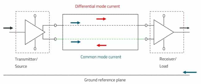
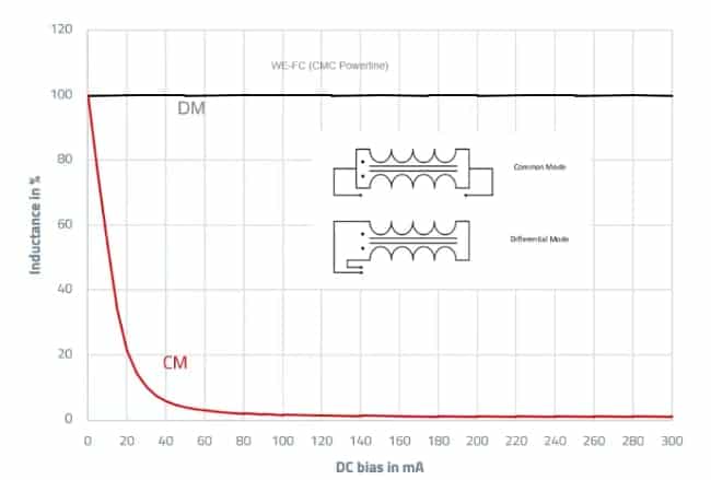
A common mode choke has at least two windings on a shared core. In common mode, the currents in both windings generate co‑directional magnetic fields, increasing flux and presenting high impedance that blocks common‑mode noise. In differential mode, currents produce opposing magnetic fields that largely cancel, leaving the choke with very low impedance for the desired signal. This field cancellation explains why, under normal operating conditions, common mode chokes do not saturate even at high differential‑mode currents, unlike single‑winding inductors.
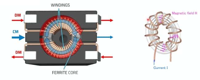
Measurement data presented in the webinar show that common mode chokes saturate quickly when driven in pure common mode, but in differential mode the effective flux remains near zero and saturation is negligible. Given that common‑mode noise currents are usually only in the microampere to milliampere range, this saturation behaviour rarely poses a design problem.
Winding styles and parasitics
Two main winding styles are used in common mode chokes:
- Bifilar (or multifilar) winding: windings wound side by side, giving very small stray fields and low leakage inductance.
- Sectional winding: each winding occupies a separate half of the core or separate bobbin chambers, increasing stray fields and leakage inductance.
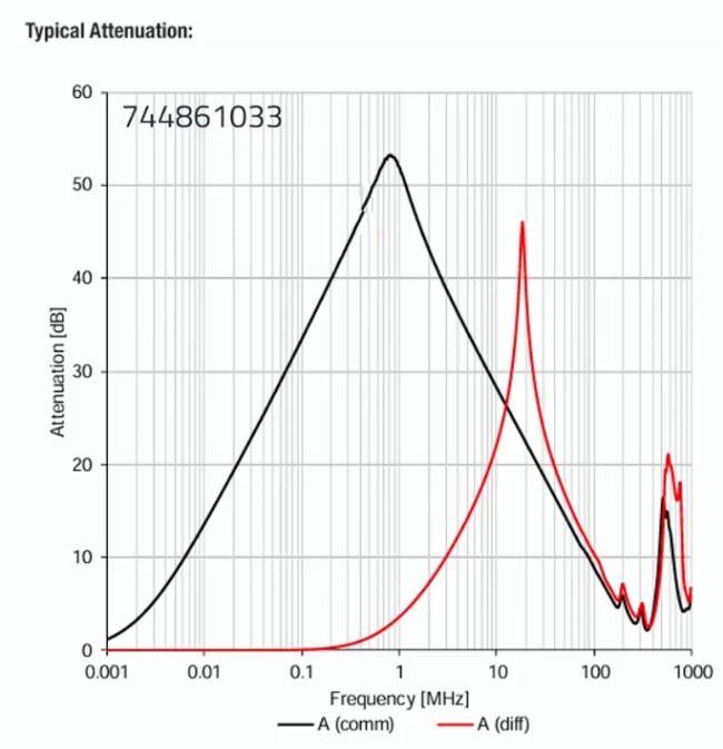
Closer coupling between windings (bifilar) minimizes the stray field and leakage inductance, which is desirable in many data‑line chokes where low differential‑mode impedance is required. Sectional winding, used widely in mains chokes, increases leakage inductance and parasitic capacitances, which can be exploited to provide some differential‑mode attenuation at higher frequencies without significantly affecting the fundamental mains frequency (50/60 Hz).
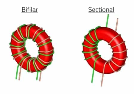
Design examples show that even with identical nominal inductance and core material, different winding geometries lead to significantly different attenuation curves versus frequency. Frame‑core chokes with separated chambers reduce parasitic capacitances and shift resonance to higher frequencies; toroidal chokes may have different parasitic distributions. For power‑line filters, the combination of winding style, parasitic capacitances, and leakage inductance can be tuned so that a single common mode choke attenuates both common‑ and differential‑mode noise, potentially eliminating the need for a separate differential‑mode inductor.
Core materials and impedance profiles
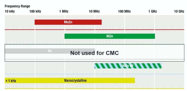
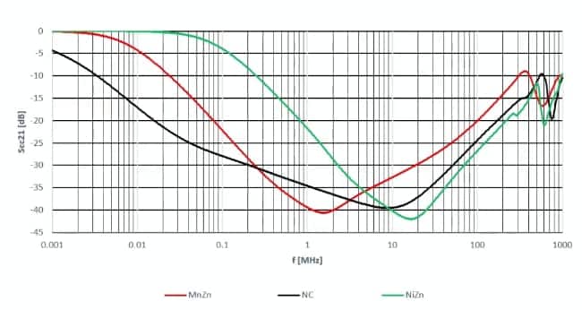
The webinar compares similar‑size toroidal common mode chokes using different core materials:
- Manganese‑zinc ferrite: best attenuation at lower frequencies, typically used for mains filters and low‑frequency noise suppression.
- Nickel‑zinc ferrite: suited to higher‑frequency noise, with resonance reaching nearly 20 MHz in the example plotted.
- Nanocrystalline cores: offer a broad useful frequency range with good temperature stability and moderate attenuation amplitude, often enabling smaller component sizes for the same inductance and performance.
Although three chokes in the example all share a nominal inductance of 1 mH, their impedance and attenuation curves differ significantly across the frequency spectrum. The number of turns required to achieve the same inductance also differs between materials, affecting copper loss and size. This demonstrates that choosing a common mode choke purely by inductance is inadequate; designers should consult impedance or attenuation vs frequency curves and match these to the noise spectrum they need to suppress.
| Corematerial | Number of turns | Wirediameter in mm | Inductance in mH |
|---|---|---|---|
| MnZn | 12 | 0,6 | 1,00 |
| Nanocrystalline | 13 | 0,5 | 5,00 |
| NiZn | 13 | 0,5 | 0,11 |
Design‑in notes for engineers
Selecting and placing varistors
When selecting a varistor for surge protection:
- Choose the working voltage at least about 25% higher than the maximum normal operating voltage to avoid premature leakage conduction.
- Verify the maximum surge current and energy capability against the worst‑case surge (IEC 61000‑4‑5) and EFT/B test levels and the expected number of events over the product lifetime. Lifetime derating graphs in the manufacturer datasheet show the theoretical number of pulses a varistor can withstand before failure.
- For data‑line or space‑constrained designs, multilayer varistors provide smaller footprint and faster response but lower energy handling; they should be reserved for applications where surge energy is low and the primary concern is ESD and small transients.
In practice, varistors age as they are repeatedly subjected to surges: material degradation at zinc‑oxide grain boundaries weakens barrier properties, increasing leakage current over time. Engineers can monitor varistor health by periodically measuring leakage current or the I–V curve; a significant increase in leakage compared to new devices is a strong indication that replacement is advisable. Capacitance change with age is expected to be modest and primarily of theoretical interest, assuming electrode spacing remains unchanged.
Parallel connection of varistors is generally discouraged because small differences in clamping voltage and leakage current cause current to concentrate in the “weakest” varistor, which then absorbs most of the energy and fails first. Instead, designers should select a single varistor with suitable surge rating for the application or consider series combinations where appropriate and supported by datasheet guidance.
ESD suppressor selection and data‑line impact
For ESD protection on data lines:
- Prioritize low capacitance to minimize insertion loss at the data frequency and preserve eye diagrams and bit error rates. Super‑speed families are tailored for high‑data‑rate interfaces, while standard families may be acceptable for slower interfaces.
- Consider whether TVS diodes with snapback behaviour are advantageous; their lower clamping voltage at equal current improves protection but requires confidence that the additional trigger voltage is negligible relative to ESD stress levels in your application.
- For closely spaced pads or extremely compact layouts, multi‑array varistors can provide multiple protection paths in one package; improved production processes now allow these arrays to achieve lower capacitance values than earlier generations.
Insertion loss becomes especially critical for very sensitive or small‑signal data interfaces. Designers should correlate interface baud rates or spectral content with recommended capacitance ranges from the manufacturer’s tables, then validate the chosen ESD component through S‑parameter simulations or lab measurements if possible.
Common mode choke selection and data sheet interpretation
When selecting common mode chokes, engineers should:
- Define clearly whether the application is mains, DC power, data, or a mixed use case, since this determines priorities such as insulation level, leakage inductance, and differential‑mode impedance.
- Use the rated current and rated voltage parameters together with derating curves and ambient temperature assumptions to ensure the choke operates within thermal limits; for example, a choke rated at 70 °C ambient with 55 K maximum self‑heating must not exceed its maximum operating temperature when both ambient and self‑heating are summed.
- Follow IEC 60638 creepage and clearance requirements (as referenced in the webinar) for mains chokes: for 230 V AC systems, typical clearances of about 2.5 mm and creepage distances between roughly 1.25 and 4 mm are required depending on insulation material and pollution degree. Sectional winding supports these distances more easily than bifilar winding.
IEC 60938 Safety Requirements
| Mains supply nominal voltage line-to-neutral | 150 V | 300 V | 600 V | 1000 V |
|---|---|---|---|---|
| AC voltage | 150 V | 300 V | 600 V | 1000 V |
| DC voltage | 250 V | 450 V | 900 V | 1500 V |
| Between live parts of different polarity | 1,5 mm | 2,5 mm | 3,0 mm | 5,5 mm |
Designers should avoid comparing components solely at a single inductance value from datasheets. Instead, it is better to examine plots of inductance vs frequency and impedance/attenuation vs frequency, ensuring the nominal inductance is defined in a frequency region where test equipment accuracy is acceptable and where frequency effects are minimal. Manufacturers often reference IEC test frequency recommendations (e.g., using 10 kHz for inductors of 1 mH and above), which help align measurements across different product families.
Winding style, leakage inductance, and mixed filters
For power‑line filters:
- Sectional winding style creates higher leakage inductance and parasitic capacitances, contributing useful differential‑mode attenuation at frequencies much higher than 50/60 Hz while meeting creepage and clearance requirements. This can reduce or eliminate the need for separate differential‑mode chokes in some designs.
- The desired mains signal at 50/60 Hz is unaffected because the differential‑mode attenuation begins only at significantly higher frequencies (e.g. in the 100 kHz to 1 MHz range, as shown in attenuation curves below).
- Frame‑core chokes with separated chambers reduce parasitic capacitances and shift resonance to higher frequencies, tailoring the filter’s band of maximum attenuation. Engineers can use winding geometry and parasitics intentionally to place resonances where the dominant noise energy lies.
For data and DC line filters:
- Bifilar winding minimizes leakage inductance and parasitics, keeping differential‑mode impedance low; this is important in data‑line chokes to avoid degrading signal rise times and introducing jitter.
- In DC‑line chokes, both common‑mode and differential‑mode impedances can be beneficial, as high impedance in both modes helps reject conducted noise in low‑power lines, provided voltage drop due to DC resistance remains acceptable.
- Recommended PCB layout places the common mode choke as close as possible to the connector, isolating the PCB from external noise sources and preventing internal noise from coupling onto cables. Example implementations in LED matrices show flicker problems resolved by adding an appropriately selected DC common mode choke near the output connector.
Lifetime, ageing, and portfolio updates
The webinar highlights ongoing portfolio evolution and reliability improvements:
- Würth Elektronik’s THT varistor series have had their maximum operating temperature upgraded from 85 °C to 105 °C, enhancing robustness for high‑temperature environments according to manufacturer datasheets.
- The VS multilayer varistor series has been converted to lead‑free versions following a product change notice (PCN), aligning with environmental and regulatory expectations.
- New common mode choke variants include a CNSW series size tailored for CAN bus applications and expanded DC choke families with additional sizes and packages, plus an upcoming CNB HV series with higher voltage ratings up to approximately 1,000 V AC and 1,250 V DC and planned certification by VDE and another safety agency.
For long‑life applications, engineers should combine datasheet lifetime derating graphs with their specific surge/ESD environment and consider periodic leakage‑current monitoring on varistors and similar devices during maintenance intervals.
Technical highlights summary table
The following table summarizes some of the key component characteristics discussed in the webinar, as a quick design reference. Exact numerical values should be taken from the relevant manufacturer datasheet.
| Component type | Key function | Strengths in practice | Limitations / caveats |
|---|---|---|---|
| THT disc varistor | Surge clamping on mains/DC | High energy handling, wide voltage range, simple integration | Higher capacitance, ageing increases leakage |
| Multilayer SMD varistor | ESD/surge on data & low‑power lines | Fast response, low capacitance, small footprint | Lower surge current and energy capability |
| TVS diode (unidirectional) | ESD/surge, especially low‑voltage rails | Sharp breakdown, precise clamping, SMD form factor | Narrow clamping region, some variants show snapback |
| TVS diode with snapback | Improved ESD clamping | Lower clamping voltage at same current, better protection | Needs extra trigger voltage, behaviour PCB‑dependent |
| Common mode choke, sectional winding | Mains and power filters | High common‑mode impedance, useful differential‑mode attenuation via leakage, good insulation | Larger stray field, higher parasitics |
| Common mode choke, bifilar winding | Data and low‑voltage filters | Low leakage inductance, minimal differential‑mode impedance, compact | Less suited to meeting large creepage/clearance distances |
| Standard capacitance ESD family | General‑purpose interfaces | Robust protection for moderate data rates | Higher insertion loss at high frequencies |
| Super‑speed ESD family | High‑speed serial links | Minimal insertion loss, preserved signal integrity | Lower energy handling, careful layout required |
All performance values and limits in this table are intended only as qualitative guidance; exact ratings depend on specific series and part numbers according to manufacturer datasheets.
Conclusion
After working through this webinar’s content, a design engineer or component buyer should be able to map real‑world surge, EFT, and ESD environments onto suitable varistor and TVS families, understand how common mode chokes differentiate between noise modes and desired signals, and interpret datasheet parameters such as breakdown voltage, rated current, inductance vs frequency, and creepage/clearance distances in a safety and EMC context. By paying attention to winding style, core material, parasitic capacitances, and placement on the PCB, engineers can turn common mode chokes from generic catalogue inductors into carefully tuned filter elements that address both common‑ and differential‑mode noise at relevant frequencies.
For practical next steps, designers should review manufacturer application notes on mains filter design and common mode chokes, consult updated series information (such as new CAN‑oriented chokes and high‑voltage variants), and cross‑check lifetime and thermal derating curves against their expected surge environment and ambient temperatures. Purchasers can use this understanding to distinguish between components chosen purely on inductance or voltage rating and those selected for frequency‑appropriate impedance profiles and lifetime performance, improving both EMC compliance and long‑term reliability of the systems they support.
FAQ
Surge (IEC 61000‑4‑5) is a high‑energy, low‑frequency overvoltage event typically associated with lightning and large switching transients. EFT/B (IEC 61000‑4‑4) consists of many lower‑energy, high‑repetition pulses caused by switching inductive loads in industrial environments. ESD (IEC 61000‑4‑2) features very high voltage but relatively low energy and low repetition, arising from contact or air discharges between charged bodies. These differences in waveform shape, energy and repetition are critical when specifying protection components and test levels.
THT disc varistors are preferred in mains and higher‑energy DC applications where surge pulses can be large and the circuit has enough space for a relatively bulky component. They offer higher surge current and energy handling, plus a wider working voltage range. Multilayer SMD varistors are better suited to compact boards and data or low‑power lines, where transient energy is lower and fast response with low capacitance is more important than maximum surge capability.
The working voltage should be at least about 25% higher than the maximum normal operating voltage of the circuit. This ensures the varistor remains in the leakage region under normal conditions and only begins to conduct significantly when an overvoltage occurs. Designers should also verify that the maximum surge current and energy ratings match the worst‑case surge and EFT test levels and expected number of events over the product lifetime.
In low‑inductance ESD suppressors, capacitance largely determines impedance and thus insertion loss at high frequencies. Higher capacitance lowers the resonance frequency and increases insertion loss above that point, which can distort eye diagrams and increase bit error rates on interfaces such as USB or Ethernet. Low‑capacitance TVS diodes or multilayer varistors are therefore preferred for high‑speed lines to maintain signal integrity while still providing adequate ESD protection.
A common mode choke has at least two windings on a shared core. In common mode, currents in both windings flow in the same direction and their magnetic fields add, creating high impedance to block noise. In differential mode, currents flow in opposite directions and their fields cancel, leaving low impedance for the desired signal or power. This field cancellation means that, under normal operating conditions, common mode chokes do not saturate like single‑winding inductors carrying the same differential‑mode current.
Bifilar or multifilar winding places windings side‑by‑side, minimizing stray fields and leakage inductance, which is ideal for data‑line chokes where low differential‑mode impedance is required. Sectional winding separates windings into distinct chambers, increasing leakage inductance and parasitic capacitances, which can be exploited to attenuate high‑frequency differential‑mode noise in mains filters. Core material (manganese‑zinc, nickel‑zinc, nanocrystalline) sets the effective attenuation bandwidth and resonance behaviour, so engineers should compare impedance or attenuation vs frequency curves rather than relying on inductance alone.
Common mode chokes should be placed as close as possible to connectors and system boundaries to prevent noise from entering or leaving the PCB. Varistors and TVS diodes used for surge and ESD protection should also be located near the source of overvoltage events, such as input connectors or exposed pins, with short traces to minimize parasitic inductance. This placement strategy helps contain interference at the edges of the system and reduces stress on downstream components.
How‑to: Combine varistors, TVS diodes and common mode chokes in a mains EMI filter
- Step 1 – Define EMC and safety requirements
Determine required surge, EFT and ESD immunity levels, conducted emission limits and applicable insulation standards for the mains filter.
- Step 2 – Select a suitable THT varistor for surge protection
Choose a disc varistor with working voltage above the mains peak, appropriate surge and energy ratings, and a package that meets creepage and clearance requirements on your PCB.
- Step 3 – Add TVS or multilayer varistors for ESD and fast transients
For sensitive low‑voltage nodes or data ports, select low‑capacitance TVS diodes or multilayer varistors to handle ESD and fast transients without degrading signal integrity.
- Step 4 – Choose a common mode choke tuned to the noise spectrum
Select a sectional‑wound mains common mode choke whose attenuation vs frequency curve covers the dominant common‑ and differential‑mode noise frequencies while leaving 50/60 Hz unaffected.
- Step 5 – Complement with X and Y capacitors and discharge resistor
Add appropriately rated X capacitors across line and Y capacitors to protective earth, together with a discharge resistor, following manufacturer application notes for single‑phase line filters.
- Step 6 – Place components and verify performance in EMC testing
Arrange the fuse, varistor, common mode choke, capacitors and resistors in a compact mains filter section, then validate performance against surge, EFT, ESD and conducted EMI tests, adjusting values as needed.
Source
This article is based on engineering information presented in a Würth Elektronik technical webinar titled “EMC Design Fundamentals: How to Use Varistors and Common Mode Chokes Safely,” including the accompanying transcript and linked application documentation from the manufacturer.
References
- EMC Design Fundamentals: How to Use Varistors and Common Mode Chokes Safely (Würth Elektronik YouTube webinar)
- ANP015 – 1‑Phase Line Filter Design (Würth Elektronik application note)
- Catalogue and tutorial – Common Mode Chokes (Würth Elektronik)
- Mains Filter Guide poster (Würth Elektronik)
- ANP146 – Theoretical background and practical applications of WE‑CMDC common mode chokes (German)
- Würth Elektronik eiSos – Product overview

