
Source: Würth Elektronik blog
Electromagnetic (EM) radiation from inductors in DC/DC converters is no triviality — especially when considering the type and proximity of surrounding components and their susceptibility to magnetic coupling. In this post, we will discuss EM radiation as it pertains to unshielded, semi-shielded, and shielded inductors. We will also cover how EM radiation changes according to different influences.
Power Inductors and Electromagnetic (EM) Radiation
Power inductors in switch mode power supplies (SMPS) can be made of various core materials and different types of windings (coils). Inductors can also be classified into three types:
- Unshielded
- Semi-shielded
- Shielded
Different types of inductors have advantageous and disadvantageous characteristics that permit or limit their range of application.
Due to the switching action in SMPS, AC voltage/current is produced over the inductor. Since an inductor can, in effect, operate as a transmitting loop antenna, the electromagnetic radiation depends on a number of factors, including:
- Source properties (such as core material)
- Shielding material
- Orientation of the start of the winding
Electromagnetic radiation of an inductor in the low frequency spectrum range (100 kHz to 30 MHz) — which is caused by the switching frequency and harmonics — is dependent on both whether the inductor is shielded and the winding properties. On the other hand, in the high frequency spectrum range (30 MHz to 1 GHz) — where emissions are caused by ringing frequencies and their harmonics — the electromagnetic radiation is more dependent on the shielding characteristics of the core material, switching frequency, and transitions of the switching converter.
How Electromagnetic Radiation Works
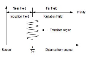

Fig.1. Near and far-field region(s) spread spectrum
The inherent design and operation of an inductor in DC/DC converters leads to unfavorable attributes, comparable to those of a loop antenna. The AC voltage and current in the inductor produces electric (E-field) and magnetic (H-field) fields, which propagate away from the source at right angles to one another.
Near to the loop antenna (source), the characteristics of the fields (E and H) are determined by the behavior of the source characteristics (switching frequency, transitions). However, far from the source, the properties of the field are determined by the medium through which it propagates. These separate yet interconnected phenomena can therefore be divided into two regions: the near-field and the far-field (as shown in Figure 1). The area within λ /2π of the source is defined as the near-field, whereas anything further than this is defined as far-field radiation.
In the near-field, the E- and H-fields must be considered separately, as the ratio between the two fields is not constant. The ratio E H ൗ is also called wave impedance. However, in the far-field, these fields combine to form a plane wave. That is why individual electric (E) and magnetic (H) fields are only discussed in the context of near-field. If the source has high current and low voltage, the magnetic field is said to be dominant, whereas if the source has low current and high voltage, the electric is said to be dominant.
For a loop antenna, the magnetic field near the source is high, resulting in a low wave impedance near the antenna. As the distance from the source increases, the magnetic field declines, simultaneously generating an electric field perpendicular to the direction of the H-field. The magnetic field attenuates at a rate of ( 1 r ൗ ) 3, and the electric field attenuates at a rate of ( 1 r ൗ ) 2, when moving away from the source where r is the distance. For a straight wire antenna, the wave impedance is high, which is why the electric field is dominant near the source and the attenuation characteristics are entirely opposite to that of loop antenna.
EM Radiation Behavior of Unshielded, Semi-Shielded, and Shielded Inductors
As engineers have become more mindful of electromagnetic radiation as a source of potential EMI, component manufacturers have responded by offering ranges of inductors that are shielded and semi-shielded in addition to conventional unshielded inductors.

Shielded inductors are manufactured to fully encapsulate the coil in a form of magnetic shielding. With unshielded inductors, the coil windings are typically exposed or otherwise magnetically not shielded. These are generally the worst offenders from an EMI perspective due to the unhindered propagation of EM fields. In semi-shielded inductors, magnetic materials are usually glued over the exposed windings with epoxy resin.
Each type of inductor has its own advantages and disadvantages. The main advantage of the shielded inductor is its relatively low emissions when compared to semi-shielded or shielded inductors.
But, as most electrical engineers know, a fine balancing act must be maintained when a new design is in development. Increasing a desirable characteristic can often increase undesirable characteristics, which are ultimately restrained by the overall project requirements. One of those restraints is inescapably size.
Shielded inductors, when compared to the same inductance value required of unshielded inductors and of the same dimensions, have lower DC-resistance and lower saturation. Naturally, this would direct the less experienced engineer to select an unshielded inductor, which is smaller and has higher saturation current capability. But this will ultimately lead to a myriad of electromagnetic interference and compatibility issues that cannot be compromised.
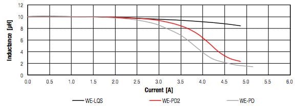
Würth Elektronik is one of the few companies to offer semi-shielded inductors that walk the fine line balancing space requirements, electrical characteristics, and EMI. Semi-shielded inductors are particularly suited to applications where components close to the inductor are not severely sensitive to radiation. The excellent saturation characteristics of the WE-LQS semi shielded inductor size 8040 ( 744 040 841 00) are presented in Figure 5 and compared with shielded inductor WE-PD size 7345 ( 744 777 10) and unshielded inductor WE-PD2 size 7850 ( 744 775 10).
EM Radiation due to the Influence of the Start of the Winding in an Inductor
One EMI consideration that can easy be overlooked is the orientation of the start of the coil winding. The “dot” on the inductor package represents the start of winding. It is important to connect the dotted end of the inductor closest to the switch node, as this is the end that will undergo the most dV/dt and thus generate the most interference. In this way, the AC flux from switch node switching will be shielded by the outer windings. If the non-dot end is connected to the switch node, AC flux voltages will be present on the outside winding layer, which can cause unacceptable levels of electric or capacitive coupling.
Magnetically shielded inductors are effective at shielding H-field dominant radiation, but they may not be able to shield E-field dominant radiation in all conditions. Effective E-shielding depends on the material properties and complex permeability. The higher the thickness and permeability of the core material, the more effective the inductor will be at shielding the E-field.
As an example, the E-field emissions of a Würth Elektronik shielded inductor was measured with a WE-LHMI ( 744 373 680 22). The transistor of the converter was operating at 400 kHz, producing the fundamental resonance and subsequent harmonics. The spectrum clearly shows that emissions from the inductor re up to 8 dB lower when the dotted end of the inductor is connected to the switch node (Figure 3a). It is, therefore, highly recommended to use the inductor in the correct orientation. The H-field emissions, however, are unaffected by the change of orientation of the inductor (Figure 3b).
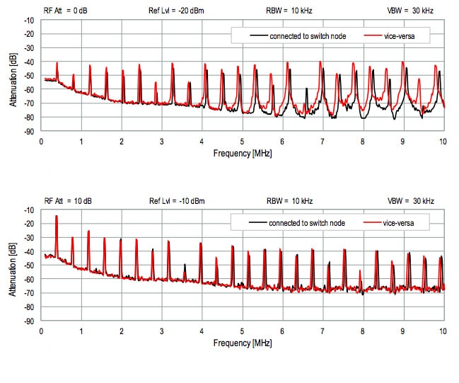

Fig.3. E-field (3a top image) and H-field (3b bottom image) of the inductor’s start of winding connected to the switch node and vice-versa
EM Radiation due to the Influence of Switching Transitions
There cannot be electromagnetic interference if the source, medium, or the victim is not present. As switching frequencies increase, DC/DC converters also employ faster rise and fall times of the switching device to keep switching losses low. But this creates steep switch-node transitions, accompanied by switch-node ringing and spikes.
Because of switch node ringing, fast transitions, and high switching frequency, it is necessary to choose an appropriate inductor for achieving EM compatibility. Typically, the ringing frequency is in the 100 to 200 MHz range. The effectiveness of attenuating emissions at these frequencies very much depends on the inductor’s properties, especially the core material and thickness.
The effect on the radiation of H and E-fields when changing the core material may be seen in Figure 4a and Figure 4b.
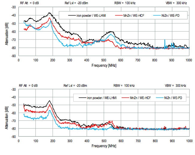

Fig.4. H-field (4a top image) and E-field (4b bottom image) comparison of iron powder (WE-LHMI), Mn-Zn (WE-HCF) and NiZn (WE-PD) core material.
The DC-DC converter used for the testing is switching at 400 kHz, and the ringing frequency on the switch node is about 180 MHz. As demonstrated, an inductor with a NiZn core ( WE-PD 744 771 402 2) is much more successful at limiting H- and E-field radiation at higher switching frequencies than an inductor with MnZn core ( WE-HCF 744 363 022 0).
Clearly, EM radiation is an important consideration in terms of potential EMI and other issues pertaining to power management. That’s why it’s so crucial to select the right power inductor for your design.
How Shielding Materials Affect Electromagnetic Radiation and the Effectiveness of a Power Inductor
Every core material has inherent advantages and disadvantages that are particularly suited to a specific application. In these circumstances where a core material cannot be substituted, external solutions may be necessary to mitigate emissions.
For example, inductors made of iron powder/metal alloy core material have excellent saturation characteristics and can be made in extremely small sizes, but they have limited shielding characteristics at frequencies above 1 MHz. So to shield the emissions from the ringing frequency caused by a fast switching transition time, external shielding may be required to ensure electromagnetic compatibility.
Metal and magnetic shielding solutions can be optimized based on the application. Metal shielding materials are made of copper, aluminum, metal alloys, and composite mixtures. Metal shielding usually consists of an enclosure that is attached over the source to reflect or absorb the noise. The thickness and type of material can be chosen based upon shielding effectiveness, frequency, and cost.
Interestingly, some iron powder inductor manufacturers are integrating a metal bridge on the top of the inductor to improve shielding performance. However, this approach is less advantageous than it may first appear. These inductors are not as flexible to design and emission requirements, as they have a limited effect at a constrained range of switching frequencies and fixed source properties.
Alternatively, magnetic shielding can be achieved using magnetic materials or µ-metals and their effectiveness are dependent on material permeability, impedance, and thickness.
Effect of Shielding in the Near-Field
The switch node ringing frequency on one demo-board is ≈130 MHz, and on the other demo-board it is ≈ 180 MHz. Since the advantages of iron powder and metal alloy inductors cannot be compromised most of the time, Würth Elektronik offers a huge variety of metal and µ-metal shielding materials, such as copper tape, various composite metal shielding cabinets with and without vents, NiZn and ferrite plates, and more.
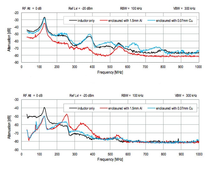

Fig.5. H-field (5a top image) and E-field (5b bottom image) comparison of iron powder (WE-LHMI) without additional shielding, with 1.5mm Aluminum enclosure and 0.07mm copper tape.
These products offer flexible and adaptable solutions that are suitable for specific design restraints and can be selected for the particular range of frequencies where attenuation is required (Figure 5a). For example, the effectiveness of metal shielding of a Würth Elektronik WE-LHMI iron powder inductor is demonstrated by a 10 dB reduction in E-field emissions (Figure 5b).
Effect of Shielding in the Far-Field
The effectiveness of shielding is not only limited to near-field radiation. Notable reductions in far-field emissions can also be achieved using metal and ferrite solutions.
The same demo-board was tested in the EMI chamber for far-field radiation.
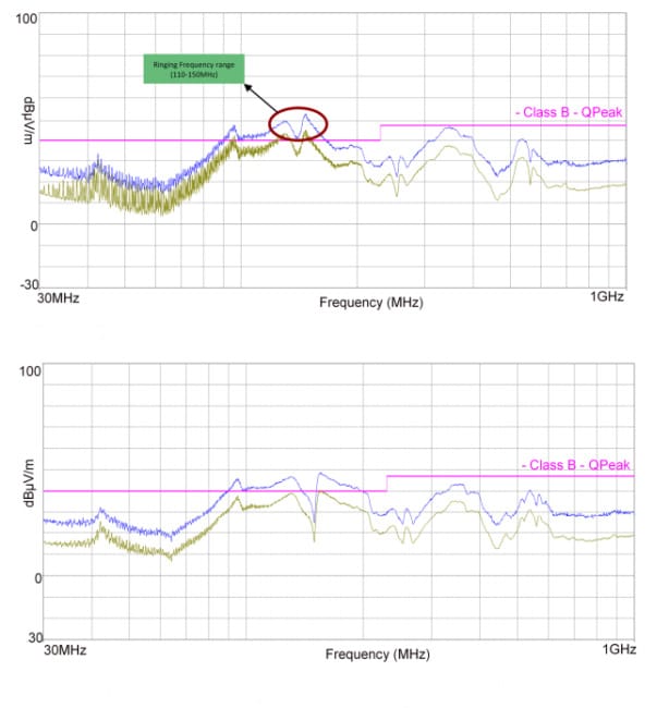

Fig.6. Far-field electro-magnetic radiation of the system where iron powder inductor is parts of it (6a top image), or Aluminum enclosure on the inductor (6b bottom image)
The value of enclosing an iron powder core inductor with a 1.5 mm thick aluminum shield is demonstrated in Figure 6a and Figure 6b, where the ringing frequency has been substantially reduced. In addition, attenuation was also notable over the whole frequency range, including harmonics. Similarly, the addition of adding a 3 mm-thick ferrite plate has a similar effect when placed on the iron powder inductor.
Summary of EM Radiation of Power Inductors in Power Magnetics
EM radiation is an incredibly vast and intricate topic, as seemingly small variations in any one parameter can influence emission sources and therefore the near-field and far-field characteristics. The characterization of the near-field can be a complicated and lengthy process because of the necessity of many experiments and observations to fully comprehend and resolve EMI issues.
Plus, the move toward high switching frequencies for higher power densities and better efficiency — as the availability of new technologies in Mosfets becomes readily available (GaN, SiC) — further necessitates the consideration and control of emissions. When switching at higher frequencies, the usual approach for power magnetics is no longer valid.

