




Resistors are passive components that convert electrical energy into heat while providing a precise impedance to current flow. They exist in an extremely wide variety of constructions, materials, and package formats to cover everything from precision instrumentation to high‑energy pulse applications.
Key Takeaways
- Resistor types vary in construction and functionality, impacting precision, power handling, and environmental stability.
- Main resistor categories include fixed, variable, and non-linear types, each serving specific circuit roles.
- Key construction elements like substrate, resistive film, and terminations are crucial for performance.
- Resistor packaging affects integration, cooling, and application suitability in circuits.
- Understanding resistor types construction and features enables optimized selection for specific applications.
Resistors in this overview are considered as discrete components used in power electronics, precision measurement, automotive and general‑purpose electronics rather than integrated on‑chip resistors. This article focuses on how construction and packaging map to application requirements so design engineers can select the most suitable technology for long‑life, reliable circuits.
Fundamentals of Resistor Types and Construction
A resistor is characterized at the most basic level by its nominal resistance, permissible tolerance, temperature coefficient (TCR), and power/voltage ratings. The way these parameters are achieved and maintained over lifetime is predominantly defined by the internal construction and materials used.
Key construction archetypes are:
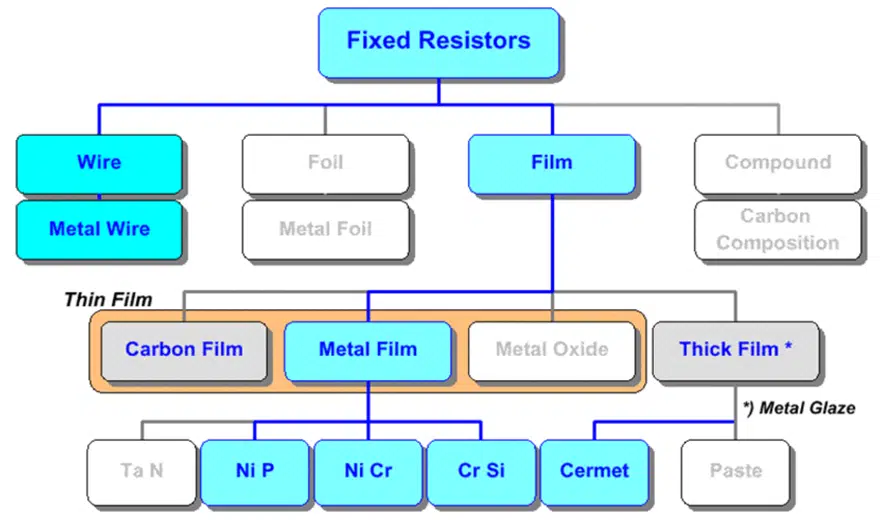
- Film resistors, where a resistive film is deposited on an insulating substrate and trimmed to value (thin, metal film, thick film, metal oxide, metal glaze).
- Bulk/element resistors, where a metal or alloy element itself forms the resistive path (wirewound, metal element, foil).
- Composite resistors, where conductive particles are dispersed in a binder (carbon composition, some surge or non‑linear elements).
- Variable resistors, where a wiper moves over a resistive track (potentiometers, trimmers, rheostats).
Construction drives:
- Achievable precision (tolerance, TCR, tracking).
- Stability and drift over time, load and environment.
- Noise and high‑frequency behavior.
- Pulse, surge and overload robustness.
Classification of Resistors by Function
From an application perspective, resistors can be classified by their electrical function in the circuit rather than by technology alone.
Typical functional roles:
- Current limiting: series resistors protecting semiconductors, LEDs, and inputs.
- Shunt measurement: low‑ohmic elements sensing current by measuring voltage drop (current sense/shunt resistors).
- Heaters: resistors intentionally used as controlled heaters or load banks.
- Sensing and transduction: strain gauge resistors, temperature sensors (thermistors), light‑dependent resistors, magnetoresistors and emerging memristors.
Within “resistors” in the broader sense, it is also useful to separate:
- Linear resistors: Ohmic over the operating range (film, wirewound, foil, metal element).
- Non‑linear resistors: resistance depends strongly on voltage, current, temperature or light (NTC/PTC thermistors, varistors, photoresistors, magnetoresistors, memristors).
| Function | Preferred technologies | Notes |
|---|---|---|
| Current limiting | Thick film, metal film, MELF, carbon film | General biasing, LED limiting and input protection in low to mid power. |
| Voltage division | Thin film, metal film, foil, resistor networks | Requires ratio stability, low noise and good tracking over temperature. |
| Shunt current sensing | Metal element, foil, low‑inductance wirewound shunts | Very low resistance, Kelvin connections and controlled TCR for accurate measurement. |
| Heaters / load banks | Wirewound, metal oxide, metal glaze power resistors | High surface load and pulse energy handling, often chassis‑mount or cemented. |
| Surge / protection | Metal oxide, metal glaze, surge‑optimized thick film, varistors | High energy pulses, inrush and lightning; coordinated with fuses or MOVs. |
| Sensing / transduction | Thermistors, LDR, magnetoresistors, strain gauge resistors | Strongly non‑linear behavior used for temperature, light or field sensing. |
Non‑linear resistors form an important separate family used for sensing and circuit protection rather than purely linear resistance. Their resistance depends strongly on voltage, current, temperature or light, and they are covered in more detail in the “Non‑Linear Passives e‑Blog”.
Typical examples are:
- NTC and PTC thermistors, whose resistance changes steeply with temperature, used as temperature sensors and inrush current limiters.
- Metal‑oxide varistors (MOV), whose resistance decreases sharply above a threshold voltage, used in surge suppression and lightning protection networks.
- Light‑dependent resistors (LDR) and magnetoresistors, where resistance varies with light intensity or magnetic field for sensing and feedback applications.
Current sense and shunt resistors
Current sense and shunt resistors are precision low‑ohmic components used to measure current indirectly by generating a small, known voltage drop according to Ohm’s law . Their construction emphasizes controlled resistance, low temperature coefficient, minimal parasitic inductance and good thermal paths to support accurate measurement over wide current and temperature ranges.
Key parameters for shunt selection include:
- Nominal resistance value, typically in the milliohm range, chosen to balance measurement resolution against power loss.
- Tolerance and TCR, which directly translate into gain error and drift in current measurement.
- Continuous power rating and pulse/overload behavior, to withstand normal operation and fault conditions such as inrush or short‑circuits.
- Inductance and layout, important for fast current sensing in switching power converters and motor drives.
A simplified design flow for low‑side current sensing is:
- Define maximum continuous current and any short‑term overload or fault currents.
- Choose a target full‑scale voltage drop across the shunt at maximum current, often in the range of tens of millivolts (for example 50–100 mV).
- Calculate the required shunt resistance using R=V/I and check continuous power P=I2R against available shunt ratings with derating margin.
- Select shunt technology (metal element, foil or low‑inductance wirewound) based on required accuracy, frequency response and mechanical format.
- Lay out the PCB with wide copper traces, Kelvin sense connections and good thermal spreading to minimize additional resistance and temperature gradients.
For a detailed step‑by‑step design procedure, see the dedicated [Shunt Current Sense Resistor] application guide linked at the end of this article
Fixed Resistors vs Variable and Special Resistors
Fixed resistors provide one defined resistance value which changes only with tolerance, TCR and drift mechanisms. Variable and special resistors allow electrical adjustment or have specifically engineered non‑linear behavior.
| Category | Examples | Key Features | Typical Uses |
|---|---|---|---|
| Fixed linear resistors | Thick/thin/metal film, wirewound, foil | Single value, stable over time and environment range | Biasing, dividers, filters, terminations |
| Variable resistors | Potentiometers, trimmers, rheostats | User or factory adjustable resistance via mechanical wiper | Calibration, volume/tone control, set‑points |
| Non‑linear resistors | NTC/PTC, LDR, varistors, magnetoresist | Resistance strongly function of T, light, voltage or field | Sensing, surge suppression, protection, feedback |
| Current sense / shunt | Metal element, foil, low‑inductance wirewound shunts | Very low resistance, Kelvin terminals, controlled TCR and inductance | Accurate current measurement in power converters, battery packs and motor drives. |
SMD, Through‑Hole, Power and Network Packages
Packaging defines how a resistor is mounted, cooled and integrated into the circuit.
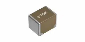
- SMD chip: Rectangular ceramic body with terminations at the ends, suitable for automated assembly and high‑frequency operation.
- MELF: Cylindrical metal‑electrode leadless format with continuous current path and superior pulse capability vs rectangular chips of equivalent footprint.
- Through‑hole axial/radial: Leads for insertion into PCBs or chassis, often larger bodies for power resistors.
- Chassis‑mount/power blocks: Metal‑cased resistors bolted to heatsinks or chassis for high power dissipation.
- Network/array: Multiple resistors in a common SMD or SIP/DIP package with defined topology and matching characteristics.
| Package family | Mounting | Typical power range per element | Advantages | Constraints |
|---|---|---|---|---|
| SMD chip | Surface | <0.01 W to ~2 W | Compact, low parasitics, automated assembly | Limited surge, small creepage |
| SMD MELF | Surface | Similar to chips, better pulse | Excellent pulse load and surface load capability | Rolling risk, special placement |
| Axial/radial THT | Through‑hole | 0.125 W to >5 W | Robust, higher voltage, easy manual placement | Larger footprint, extra assembly |
| Chassis‑mount | Bolted | Up to kW with cooling | Very high power and energy handling | Requires heatsink, mechanical design |
| SMD resistor array | Surface | Similar to chip per element | High density, good ratio tracking | Limited surge, derating interactions |
| SIP/DIP networks | Through‑hole | Up to ~0.25 W/element | Easy bus termination or pull‑ups | Package parasitics, size |
General Film Resistor Concept
Film resistors form the dominant volume technology for general‑purpose applications. A resistive film is applied on an insulating substrate and structured into a serpentine track between terminations.
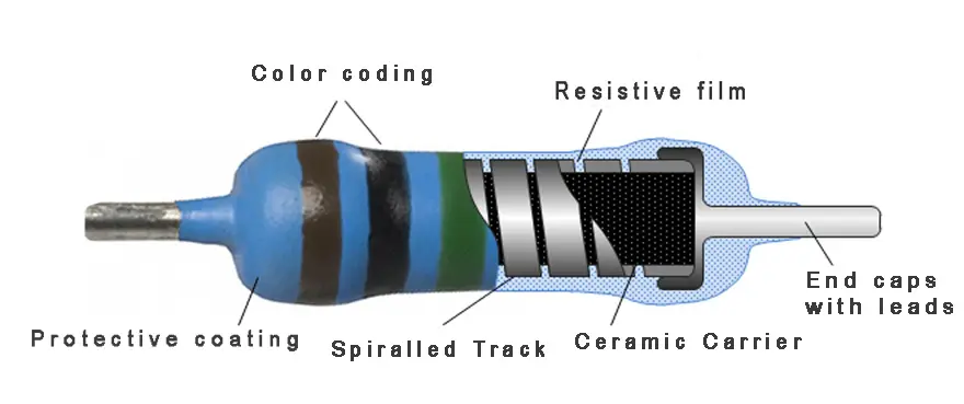
Core elements:
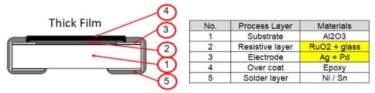
- Substrate: Ceramic (typically alumina) providing mechanical support and insulation.
- Resistive film: Material defining resistance and TCR (metal alloys, metal oxides, thick‑film pastes).
- Patterning/trimming: Laser trimming or etching to adjust resistance and linearize behavior.
- Terminations: Inner conductors, barrier layers and solderable plating (e.g. Ni barrier + matte Sn).
- Coating/passivation: Glass, epoxy or polymer protecting the resistive element from environment.
Film resistor design balances:
- Film thickness and sheet resistance to achieve desired value range.
- Track geometry for power density, voltage gradient and inductance.
- Material selection for noise, stability and moisture performance.
Thin and Metal Film Resistors – Overview
Thin film (often called metal film in chip format) uses a very thin, sputtered metallic alloy film, typically nickel‑chromium or related alloys. Film thickness is about three orders of magnitude lower than thick film, yielding a highly uniform, dense resistive layer.
Key manufacturing aspects:
- Inner conductors are screen‑printed and fired on ceramic substrate.
- Resistive film is sputtered under tightly controlled conditions from alloy targets.
- Patterning may use photolithography and laser trimming for precise geometry and resistance.
- Nickel barrier and solderable plating form the external terminations.
Performance characteristics:
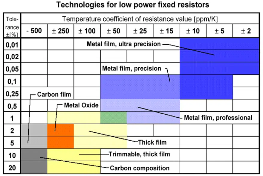
- Very low TCR and tight tolerance capability due to material uniformity and precision trimming.
- Low noise and excellent long‑term stability under load vs thick film.
- Better high‑frequency behavior thanks to uniform, continuous film and controlled geometry.
Thin film vs thick film trimming:
- Thin film’s metallic alloy conducts heat well, so laser trimming affects only a narrow zone with minimal microcracking.
- This results in lower excess noise and improved stability after trimming compared to glass‑like thick film materials.
Thick Film Chip and Network Resistors – Overview
Thick film is the most widespread technology for general‑purpose SMD resistors and arrays. The resistive element is a screen‑printed paste containing conductive particles (e.g. RuO₂‑based), glass frit, resins and solvents.
Process outline:
- Thick film paste is screen‑printed onto alumina substrates at locations defined by the stencil.
- After printing, the layers are dried and fired at high temperature to sinter the glassy matrix and anchor it to the substrate.
- Elements are trimmed by laser to final value, then covered by passivation and finished with terminations.
Behavioral characteristics:
- Wide resistance range, including very high values that are difficult for thin film.
- Inherent moisture robustness due to glass‑like fired network, though nichrome thin film with special processing or TaN can approach this.
- Higher noise and larger drift under environmental and electrical stresses because of granular, random conduction paths and trimming microcracks.
Pulse capability:
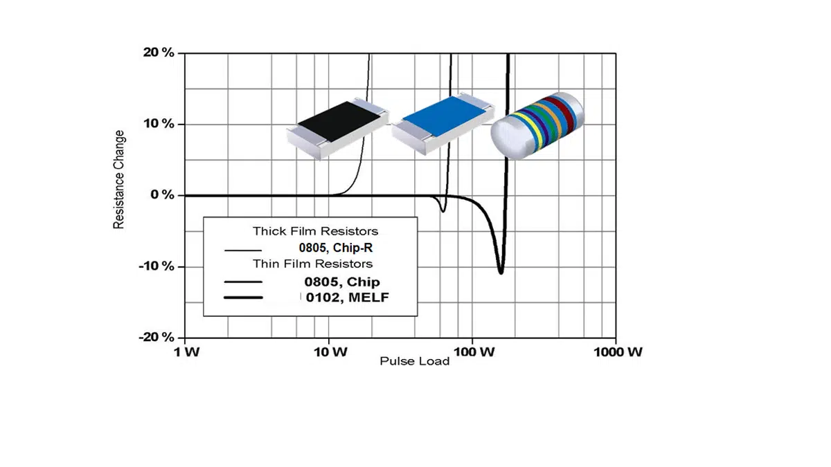
- Thick film typically handles very short pulses (<100 µs) better, while thin film is superior for longer pulses with controlled energy.
- MELF implementations further extend pulse and surface load robustness compared to rectangular chips.

Carbon Film and Carbon Composition Resistors – Overview
Carbon film and carbon composition represent older yet still relevant resistor classes for certain robustness or surge applications.
- Carbon film: A carbonaceous film is deposited on a ceramic rod and spiral‑cut to value.
- Offers medium performance for general use, with higher noise and drift than metal film.
- Costs are low, and surge robustness can be good for some designs.
- Carbon composition: Conductive carbon particles dispersed in an organic binder forming a bulk resistive body.
- Historically important for high‑energy surge and pulse applications due to distributed volume conduction.
- Today largely replaced by specialized metal oxide, thick film or wirewound alternatives, but still used where unique pulse behavior is needed.
Metal Oxide, Metal Glaze and Surge‑Resistant Resistors
Metal oxide and metal glaze resistors bridge the gap between standard film and high‑energy devices.
Metal oxide film:
- Resistive layer formed by metal oxides on a ceramic core.
- Offers superior surge and overload capability compared to standard metal film, with good stability at elevated temperatures.
Metal glaze/thick film surge designs:
- Use thick film compositions optimized for high energy absorption and surge withstand.
- Often employed as flameproof fusible resistors, in inrush limiters and protection networks.
Design trade‑offs:
- Enhanced surge capability often comes at the expense of higher noise, larger drift, or reduced precision.
- Coating and body design are key to safely containing failure energy and avoiding flaming or explosion in fault conditions.
Wirewound, Metal Element and Foil Resistors – Overview
These technologies use a bulk metallic element as the resistive path rather than a thin film.
Wirewound:
- Resistance wire (e.g. NiCr) wound on an insulating core, often with cement or protective coating.
- Very high power handling and excellent pulse/overload capability; inductive unless special non‑inductive bifilar techniques are used.
- High precision types are used in metrology; power types in load banks and braking resistors.
Metal element / shunt:
- Metal strip or stamped element with low resistance value and controlled geometry.
- Very low inductance and good thermal path, ideal for current sensing in power electronics.
Foil resistors:
- Bulk metal foil bonded to a substrate and photo‑etched into a resistive pattern.
- Offer extremely low TCR, minimal long‑term drift, and outstanding stability under load, temperature and mechanical strain.
| Technology | Precision potential | Power/pulse capability | Inductance level | Typical applications |
|---|---|---|---|---|
| Wirewound | High | Very high | Medium to high | Power, braking, high energy, precision |
| Metal element | Medium | High, especially at low R | Very low | Current sense, battery and motor drives |
| Foil | Very high | Medium, excellent stability | Very low | Precision instrumentation, references |
High‑frequency and low‑noise behavior
At high frequencies and in low‑noise analog or RF circuits, the parasitic inductance and capacitance of resistors become as important as their nominal resistance. Package geometry, resistive pattern and terminations together form an R–L–C network that can degrade impedance flatness, matching and phase response.
General trends include:
- Wirewound resistors are inherently inductive due to their coil structure and are unsuitable for many RF applications unless special non‑inductive bifilar or Ayrton–Perry winding techniques are used.
- Chip film resistors and foil resistors offer low parasitic inductance and are preferred for RF terminations, attenuators and high‑speed digital impedance control.
- Resistor networks and arrays introduce additional package‑level parasitics which must be considered in sensitive high‑frequency layouts.
Noise behavior also depends strongly on technology:
- Thin/metal film and foil resistors exhibit very low excess noise, making them well suited for precision instrumentation, low‑level signal paths and high‑resolution ADC front ends.
- Thick film and carbon composition resistors show higher excess noise due to granular conduction paths and trimming microcracks, which can be problematic in audio and low‑noise measurement circuits.
For RF and low‑noise designs, a practical rule of thumb is to prefer low‑inductance SMD film or foil resistors, keep lead lengths short, and avoid wirewound types except where their power handling is essential and inductance can be tolerated or compensated.
Potentiometers, Trimmers and Other Variable Resistors
Variable resistors provide adjustable resistance or voltage division, either set once during production or accessible to the end user.
Potentiometers (pots):
- Three‑terminal devices with a resistive track and movable wiper.
- Can function as adjustable voltage dividers or variable resistors (two‑terminal mode).
Trimmers (trimpots):
- Miniaturized potentiometers intended for infrequent adjustment, usually by screwdriver.
- Used for calibration of offset, gain, timing and set‑points.
Rheostats and power variable resistors:
- Larger variable resistors for power control in industrial and laboratory equipment.
Other variable types:
- Digital potentiometers (IC‑based), thermistors, and sensor resistors that effectively give a variable resistance under control or stimulus.
Selection considerations:
- Track technology (carbon, cermet, wirewound, conductive plastic) affects noise, wear and stability.
- Mechanical life, resolution, wiper contact stability and environmental sealing are critical for long‑term reliability.
Construction Elements: Substrate, Film, Terminations, Coating
All resistor technologies share key construction elements whose implementation controls performance.
Substrate:
- Provides mechanical support, dielectric isolation and thermal path.
- Commonly alumina for SMD chips and MELF, with higher‑performance ceramics for special parts.
Resistive element:
- Film (thin, thick, metal oxide, glaze), wire, foil or composite.
- Composition, thickness and pattern define resistance, TCR, noise and stability.
Terminations:
- Combination of inner conductors, barrier layer (e.g. Ni) and solderable outer plating (e.g. matte Sn).
- Critical for solderability, leach resistance, sulphur resistance and current distribution into the element.
Coating/passivation:
- Glass, epoxy or polymer layers for environmental protection.
- Influence moisture robustness, contamination resistance and high‑voltage behavior (creepage, partial discharge).
Mechanical features:
- Chip size or body geometry, spiral patterns, edge distances and notch shapes.
- These details determine voltage rating, power density, inductance and failure mode under overload.
Impact of Construction on Power, Voltage and Reliability
Power rating, voltage rating and reliability are all direct consequences of construction choices.
Power and surface load:
- For a given footprint, effective current path length and area define surface load capability.
- MELF resistors often support higher surface load than rectangular chips, as the current can flow around the entire cylindrical surface.
Voltage capability:
- Determined by creepage distance across the resistive pattern and through the coating, and by the dielectric strength of materials.
- Spiral geometry in axial resistors must be designed to avoid excessive voltage gradient between adjacent turns.
Stability and drift:
- Thin film designs achieve better long‑term stability, lower noise, and tighter TCR compared to thick film, mainly due to uniform metallic films and benign trimming behavior.
- Thick film offers excellent moisture withstanding due to glassy sintered structure but exhibits higher drift under load and environmental stresses.
Pulse and surge performance:
- Short‑duration pulses favor thick film and MELF constructions with robust fired or continuous paths.
- Longer‑duration pulses and continuous load often favor thin film or bulk metal designs with superior thermal conduction.
Reliability:
- Microcracks from trimming and granular conduction networks in thick film increase noise and drift, reducing precision under harsh conditions.
- Foil and high‑grade thin film maintain resistance within very tight limits over temperature cycles, humidity, and load, at higher component cost.
Standards and reliability metrics
Resistor reliability and long‑term stability are quantified using standardized tests and metrics defined by IEC, AEC‑Q200 and manufacturer‑specific qualification plans. Understanding these metrics helps translate construction choices into predictable behavior over thousands of hours of operation.
Common reliability metrics include:
- Load life, typically specified as resistance change ΔR/R after 1000 h, 2000 h or 10 000 h at rated or derated power and elevated temperature.
- Temperature cycling and thermal shock, assessing mechanical integrity of films, terminations and coatings over repeated excursions.
- Damp heat / humidity bias, important for outdoor, industrial and automotive environments where moisture diffusion affects drift.
- Sulfur corrosion tests, relevant for automotive and industrial atmospheres rich in sulphur compounds that attack silver‑based terminations.
Typical drift ranges (order‑of‑magnitude) under load‑life and environment tests are:
- General purpose thick film: a few percent ΔR/R over thousands of hours in harsh conditions, lower under benign use.
- High‑grade thin film: fractions of a percent drift, often <0.1% over specified life when correctly derated.
- Foil precision resistors: very low drift, down in the tens of ppm range for metrology‑grade components.
Designers rarely operate resistors at full rated power continuously. It is common practice to derate power above 70–85 °C ambient and in high‑reliability applications to use only a fraction (for example 25–50%) of the nominal power rating to reduce drift and failure risk.
Application‑specific selection examples
Resistor technologies and packages are not interchangeable once application constraints such as temperature, vibration and pulse energy are considered. The following examples highlight typical selections:
- Automotive power converter: General biasing and sensing networks often use AEC‑Q200 qualified thick film or MELF resistors, while battery and phase current measurement relies on metal element shunts with sulfur‑resistant terminations and robust PCB copper for heat spreading.
- Precision instrumentation: High‑grade thin film or foil resistors in SMD or network formats provide very low TCR, minimal drift and low noise, with matched ratios and Kelvin connections for reference and measurement circuits.
- SMPS PFC and braking circuits: Wirewound or metal oxide power resistors in through‑hole or chassis‑mount formats handle bleeder, snubber and braking duties where high surface load, voltage rating and surge capability are more critical than precision.
Thinking in terms of “application class” as well as value and package helps avoid under‑specified resistors in demanding environments such as under‑hood automotive, grid‑connected power systems or metrology‑grade instruments.
Modern technology trends
Resistor technology has evolved from legacy carbon composition and basic film types toward more specialized solutions optimized for precision, miniaturization and harsh environments. Many older technologies remain in use mainly for niche surge and pulse applications or in legacy equipment.
Current trends include a strong shift toward:
- High‑precision thin film and foil resistors for metrology, precision references and high‑resolution ADC front ends.
- Miniaturized high‑power SMD resistors and shunts for automotive ECUs, battery management and compact power converters, often with sulfur‑resistant terminations and extended temperature ratings.
- Integrated resistor networks and arrays providing ratio‑matched elements for dense digital, RF and mixed‑signal designs where board area and matching are critical.
Acknowledging these trends in design helps ensure that resistor selections reflect current best practices rather than historical defaults.
Conclusion
Understanding resistor construction at the level of substrate, resistive element, terminations and coating allows engineers to map application requirements directly to the most suitable technology rather than selecting parts only by value and size. By comparing film, wirewound, metal element, foil, carbon and variable resistor families across precision, power, pulse, voltage and environmental performance, designers can create robust, cost‑effective solutions with predictable lifetime behavior.
FAQ – Resistor Types and Construction
The main resistor families are film resistors (thin film, metal film, thick film, metal oxide, metal glaze), bulk metal types (wirewound, metal element, foil), carbon film and carbon composition, and variable resistors such as potentiometers and trimmers.
Resistors are commonly classified by their role as current limiters, shunt current sense elements, heaters or load resistors, and sensing or transducer elements such as thermistors, light‑dependent resistors and magnetoresistors.
Fixed resistors provide a single, stable resistance value defined by their tolerance and TCR, while variable resistors like potentiometers, trimmers and rheostats offer mechanically adjustable resistance or voltage division for calibration and user control.
Power and voltage ratings depend on current path geometry, surface load capability, creepage distances and coating design, so formats like MELF, chassis‑mount power resistors or wirewound elements can handle much higher energy and voltage than standard SMD chips.
Thin film resistors are preferred when very low TCR, tight tolerance, low noise and long‑term stability are required, whereas thick film chips are ideal for general‑purpose use, wide resistance ranges and robust short‑pulse handling.
High surge and pulse applications typically use metal oxide and metal glaze resistors, surge‑optimized thick film designs, carbon composition types or wirewound power resistors, depending on the required energy, waveform and safety behavior.
Package choice determines assembly method, cooling, voltage spacing and layout density, so designers select between SMD chips and MELF, axial or radial through‑hole, chassis‑mount power blocks and resistor networks for optimal integration and reliability.
Thin/metal film and foil resistors are preferred in low‑noise and RF designs because they offer low excess noise and low parasitic inductance, while wirewound types are generally avoided at high frequencies unless specially wound for non‑inductive behavior.
For shunt resistors, focus on low resistance in the milliohm range, tight tolerance and TCR, adequate power rating and pulse capability, and low‑inductance constructions with Kelvin sense connections and good PCB thermal design.
How to select the right resistor type and construction
- Step 1 – Define the resistor’s role in the circuit
Clarify whether the resistor will be used for current limiting, voltage division, current sensing, heating, protection or sensing, because the functional role narrows the suitable technologies and package options.
- Step 2 – Specify resistance value, tolerance and TCR
Determine the required resistance range, tolerance and temperature coefficient so you can decide if a general‑purpose thick film chip is sufficient or if a higher‑precision thin film, foil or wirewound solution is needed.
- Step 3 – Calculate power dissipation and voltage stress
Compute continuous power, pulse energy and maximum operating voltage, then select a construction and package with adequate surface load capability, creepage distance and surge robustness, such as MELF, power wirewound or chassis‑mount parts for high‑energy cases.
- Step 4 – Choose package style and mounting
Decide between SMD chip, MELF, through‑hole, network or chassis‑mount formats based on assembly method, board space, thermal path and the need for matched networks or arrays in your design.
- Step 5 – Match technology to environment and reliability targets
Consider operating temperature range, humidity, pollution and sulphur exposure, then select film, metal oxide, thick film, foil or shunt technologies with appropriate coatings, terminations, derating and, where relevant, low‑noise and low‑inductance characteristics to meet long‑term stability and reliability requirements.ility requirements.
- Step 6 – Validate pulse and surge behavior
Compare datasheet pulse curves, overload ratings and failure modes for candidate parts to ensure that short‑duration or inrush pulses are safely handled by the chosen resistor construction in the intended PCB layout.
- Step 7 – Finalize selection and document assumptions
Pick the specific series and footprint, document all assumptions on power, voltage and derating, and link to detailed technology application guides so future design updates can reuse a proven resistor selection strategy.
References
For deeper design‑level guidance and technology‑specific considerations, refer to the following complementary resources:
- Resistor, What is it? – basic introduction to resistor definition, symbols and simple applications.
- Resistor Technology Selection Guide – overview and comparative guidance on choosing resistor technologies by application and performance targets.
- High‑Temperature Applications Resistor Guidelines – design rules and derating for elevated‑temperature environments and automotive‑grade resistor usage.
- Shunt Current Sense Resistor – construction, layout and error sources for current sensing applications in power converters and battery systems.
- Sulphur‑Resistant Film Resistors – termination and material strategies for sulphur‑rich environments and industrial atmospheres.
- Thermistors Basics, NTC and PTC – fundamentals of temperature‑dependent resistors as sensors and protectors, complementing the non‑linear resistor section of this article.