


This application guide written by KEMET YAGEO provides general guidelines on selecting and validating of capacitors and MLCC (Multilayer Ceramics Capacitor) resonant solution for OBCs as well as addressing some lesser-known phenomenon with MLCCs under high AC voltages.
Key Takeaways
- This application guide covers the selection and validation of Resonant MLCC for On-Board Chargers (OBCs) in electric vehicles.
- Key benefits of MLCCs over Film capacitors include higher efficiency, miniaturization, and better performance at high frequencies.
- Class 1 MLCCs (C0G) offer superior temperature stability, low self-heating, and higher current handling compared to Class 2 (X7R).
- Design challenges for Resonant MLCCs include AC voltage/current capability, series-parallel combinations, and effective thermal mitigation strategies.
- Implementing proper thermal management is crucial for achieving reliability and efficiency in OBC designs with MLCCs.
Introduction
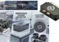
On-Board-Chargers (OBCs) are used to convert AC line voltages to DC voltages necessary for charging EV batteries. To maximize power and efficiency, designers are implementing leading-edge design topologies and components. One of these is the LLC resonant topology that utilizes a capacitor and inductor resonant circuit.
Over the past few years, designers have been moving from Film capacitors to Ceramic capacitors in the resonant circuit. By using ceramic capacitors, OBC power levels and efficiencies are reaching all-time highs. Ceramic capacitors are now transitioning from supporting components on the PCB to enabling technologies and key design considerations need to be addressed to maximize power, efficiency, and reliability of the solution.
On-Board-Chargers (OBCs)
OBCs are AC to DC converters in electric vehicles that convert the AC line voltages from the grid to DC voltages for charging the battery. The converters can operate in constant current mode or voltage mode depending on the Battery Management System (BMS) requirements and provide efficiencies above 96%. Typical OBC power levels range from 3.3kW to 22kW depending on the vehicle type.
However, designers are continuing to increase the power levels in future designs up to and beyond 30kW. At this time 3.3kW OBCs are typically used for small Battery Electric Vehicle (BEV) / Plug-in Hybrid Electric Vehicle (PHEV) while 22kW is for high-performance and commercial BEVs. For DC Fast Charging, the AC to DC converter is outside the vehicle at the charging station. Therefore, during DC Fast Charging, the OBC is bypassed and not utilized. However, the DC Fast Charger contains the LLC circuit or banks of parallel LLC circuits.
Some of the key areas of focus for designing an OBC are size, weight, efficiency, cost, and reliability. To achieve this, designers are implementing key technologies such as Wide Bandgap Semiconductors (WBG) and the LLC resonant topology.
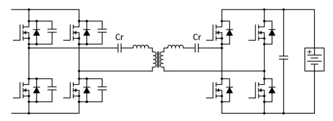
Figure 1. shows the DC-DC schematic of an OBC with a resonant tank and full-bridge rectifiers. In this schematic, the full-bridge rectifier generates a square wave into the resonant tank which outputs a resonant sinusoidal voltage that is scaled and rectified. The output capacitor filters the rectified AC voltage and outputs a DC voltage to charge the HV battery.
The use of the LLC topology for resonant converters allows for zero voltage switching (ZVS) thus drastically reducing losses at higher frequencies of operation. Typical operating frequencies for this portion of the OBC are between 50kHz – 300kHz with new technologies pushing up to 500kHz.
Resonant Capacitor Requirements
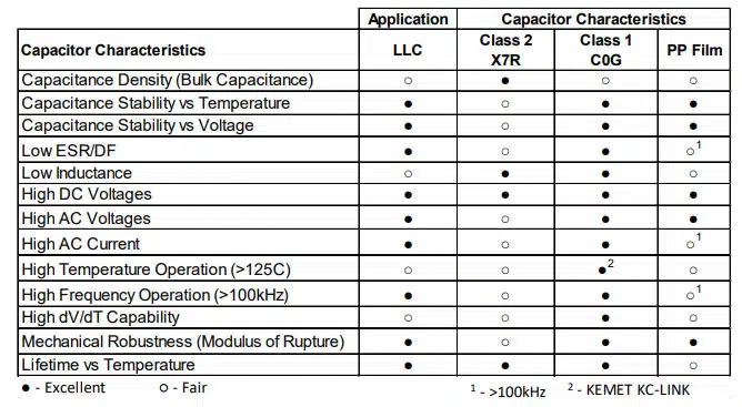
During operation, the capacitor in the LLC resonant tank will see high AC voltages, high AC currents, and ambient temperatures above 55°C depending on cooling architecture and surrounding components. In addition, the resonant frequency of the LLC circuit will need to be stable over a wide range of temperatures and voltages. The below table shows typical capacitor characteristics for resonant converters as well as the two competing technologies for the resonant capacitor.
Historically, designers have been using Film technology for the resonant capacitor but now are moving to MLCCs as the capacitor technology of choice for this critical function. The key drives for transitioning to MLCCs are miniaturization and performance at higher frequencies (>100kHz). However, the two main classes of MLCCs are Class 1 and Class 2 and the choice of class can have major consequences on the performance of the LLC.
Benefits of Class 1 vs Class 2 MLCCs
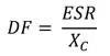
Class 1 MLCCs such as C0G are considered temperature compensating with very little change in capacitance versus temperature. The change in capacitance with temperature is linear in these paraelectric materials and does not change with voltage. The capacitance change for these dielectrics are measured in ppm per degree Celsius. Although the Class 1 MLCCs are very stable versus temperature, they have relatively low permittivity and thus lower capacitance values compared to class 2 dielectrics. However, as can be seen in Table 1 above, Class 1 MLCCs have characteristics that are far superior to any other capacitor technology that makes them ideal for resonant applications. Some of the critical characteristics for the resonant capacitor include Temperature Stability (TCC), DC and AC Voltage Stability (VCC/VCAC), Equivalent Series Resistance (ESR), Dissipation Factor (DF), and AC Ripple Current Capability:
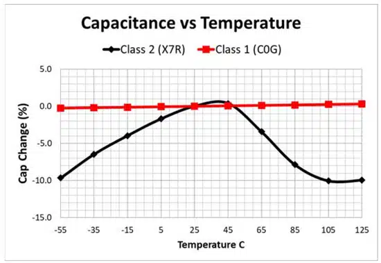
Temperature Stability (TCC): Class 1 C0G capacitors are considered ultra-stable with temperature with a maximum shift in capacitance of 30ppm/°C over the entire operating temperature range. Figure 2 below shows a comparison of TCC for C0G capacitors vs X7R.
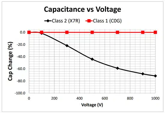
Voltage Stability (VCC/VCAC): Class 1 C0G, the capacitance change versus both DC and AC voltage is negligible and therefore has no impact on the application over the operating voltage range. However, for X7R capacitors, the VCC can be greatly impacted with applied voltage. Therefore, X7R capacitors are rarely used for resonant applications.
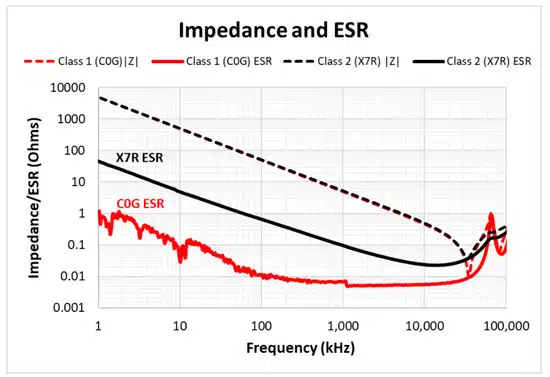
ESR, DF, and AC Current: Due to the high AC currents associated with the resonant capacitor, it is critical that the capacitors do not experience excessive heating due to I2R losses associated with higher ESR and DF. Figure 4 shows a comparison of ESR for C0G and X7R MLCCs with similar impedance characteristics. Due to the low-loss nature of the CaZrO3 dielectric material for Class 1 C0G MLCCs, the ESR is considerably lower than X7R across the entire frequency range. Notice that minimum ESR usually occurs at typical OBC operating frequency ranges of 100kHz and above. Typical DF for Class 1 C0G MLCCs is below 0.1% while Class 2 X7R is roughly 2-5%.
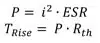
Self-heating of MLCCs depends not only on the AC current and ESR, but also the thermal resistance of the MLCC to ambient Rth. When MLCCs dissipate power due to I2R losses, the power must be dissipated through the MLCC dielectric material, electrodes, terminations, solder connections, PCB traces, and any PCB thermal mitigation. Poor thermal mitigation in PCB design leads to increased Rth resulting in increased self-heating of the MLCC. This topic will be covered in more detail in a later section of this application guide.
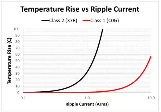
Since lower ESR and DF decrease self-heating due to fewer watts being dissipated, C0G MLCCs have much higher AC current handling capability compared to X7R. Figure 5 below shows temperature rise of C0G vs X7R capacitors over AC current. The results show that C0G capacitors can handle much higher AC currents and therefore are more desirable for resonant applications.
Considerations for Selecting MLCCs in Resonant Applications
Although this application guide covers the use of Class 1 MLCCs for resonant applications, there are still many factors to consider including: Series / Parallel combination, capacitance, tolerance, AC voltage capability, AC current capability, and thermal mitigation.
Series-Parallel Combination: Due to the high AC voltages and currents for resonant applications, almost all resonant capacitor solutions are a series-parallel combination of MLCCs. The purpose of utilizing a series-parallel combination of MLCCs is to increase AC voltage capability, AC current capability, and/or targeting a specific capacitance value. The ability to easily place MLCCs in a series-parallel combination provides designers with a very modular approach to a resonant capacitor solution and the ability to optimize maximum performance.
By adding MLCCs in series, the total voltage capability is increased but will result in a reduced overall capacitance (Figure 7). By adding MLCCs in parallel, the total current capability is increased while also increasing the total capacitance (Figure 8).
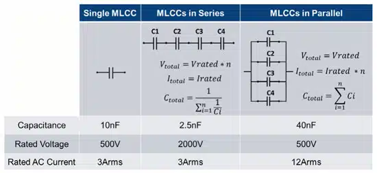
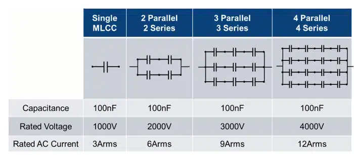
Capacitance and Tolerance: The required capacitance of the resonant capacitor will influence the necessary series / parallel combination of MLCCs as well as the tolerance for the individual MLCCs. Typically for resonant applications, MLCCs with 5% tolerance are the preferred choice for proper voltage/current balancing and targeting the resonant frequency.
AC Voltage and Current Capability: MLCCs are traditionally rated for DC voltages or currents, although they are very often used in AC applications in a wide range of frequencies.
However, most MLCC datasheets sheets do not specify an AC voltage or current since it’s highly dependent on the magnitude of the AC voltage, operating frequency and self-heating due to I2R losses.
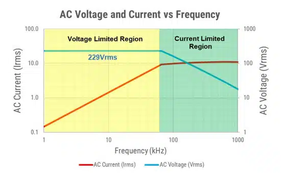
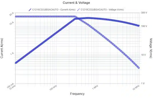
Figure 9 shows a graph of typical MLCC AC voltage (blue) and AC current (red) versus frequency along with two shaded regions: The Voltage Limited Region (yellow) and Current Limited Region (Green).
The voltage limited region is the region of the voltage and current graph where the AC current does not generate significant self-heating. In this region, KEMET has two guidelines for calculating the maximum allowable AC voltage given the DC voltage rating.
Note that these are only guidelines and do not serve as an absolute AC voltage rating of the MLCC in the application. Validation of the MLCC under full power operation is still required to assess product capability.
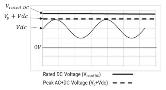
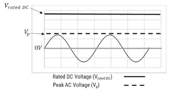
- Vrated DC: DC rated voltage of MLCC
- Vp: Peak voltage of AC waveform
- Vrms: RMS voltage of AC waveform
- Vdc: DC voltage of AC waveform (offset)
Guideline #1:
The peak voltage of the AC voltage should never exceed the rated DC voltage of the MLCCs. In this case, the peak voltage is the sum of the AC peak voltage plus the DC voltage.
VP + VDC < VratedDC
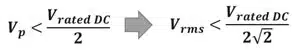
Guideline #2:
The RMS voltage of the AC voltage waveform should never exceed the rated DC voltage of the MLCC divided by two-root-two as seen below.
The current limited region is the region of the voltage and current graph in Figure 10 where the AC current generates enough I2R losses in the MLCC causing self-heating beyond the safety margin of the MLCC. KEMET’s KSIM simulation provides AC Voltage and Current versus frequency where both the voltage and current limited regions are shown. By default, the current limited region is defined as the point where the initial MLCC self-heating (ΔT) reaches 20°C and therefore the AC voltage is reduced thus limiting the AC current to not exceed this temperature. KEMET recommends that the self-heating (ΔT) be below 20°C during the first 30 minutes of operation. In addition, the max temperature of the MLCC shall be below the operating temperature for the entire lifetime of the applications. The max operating temperature of the MLCC can be found on the individual specification sheet.
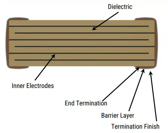
Thermal Mitigation: Class 1 MLCCs are constructed using alternating layers of ceramic dielectric and metal electrodes as seen in figure 11 below. Each layer of inner electrodes provides good thermal conductivity to the end terminations and usually MLCCs will have many internal layers. Therefore, the thermal resistance for MLCCs from the center of the chip to the termination will be very low compared to other capacitor technologies.
An often-overlooked design consideration in MLCCs for power applications is thermal mitigation. It is well known and documented with power semiconductor devices to implement thermal mitigation techniques such as thermal vias, heat sinks, and active cooling.
However, oftentimes when MLCCs are used in high power applications, thermal mitigation is not considered leading to more MLCCs to handle increased power levels or excessive temperature rise in the application.
It is therefore important to consider thermal mitigation to maximize the performance of the MLCC solution, achieve higher power efficiency, and longer-term reliability. The amount of heat (power dissipation) is dependent upon several factors such as operating frequency, RMS current, and ambient temperature.
The heat generated by the MLCC is conducted out of the MLCC primarily through the terminations, solder joints, thermal vias, heavy copper traces, and then a heat sink. Each point in the thermal pathway to ambient is an opportunity for high thermal resistance leading to poor thermal dissipation and higher overall MLCC temperature. Very little heat is dissipated through convection to ambient.
The two terminations of the MLCC may be connected to different effective thermal resistances or one may be thermally connected to a heat source like a SiC MOSFET, so a 2R model which can account for this imbalance is helpful over a single-resistor model.
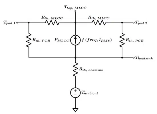
Figure 12. shows a 2R thermal resistance model for an MLCC to model the temperature rise due to power dissipation under high AC conditions. The 2R model consists of the thermal resistances of the MLCC, PCB, and heat sink as separate lumped elements.
The thermal resistance of the MLCC is defined from top of the MLCC ceramic to the terminations. The thermal resistance of the PCB is defined from the solder joint of the MLCC through the PCB traces, PCB substrate, and any thermal vias to the heat sink. The 2R model clearly shows that the temperature rise of the MLCC is not only due to the thermal resistance of the MLCC itself, but also the thermal resistance of the PCB and heat sink.
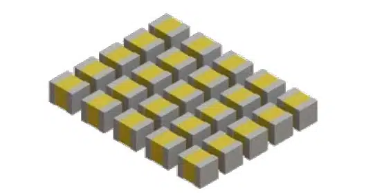
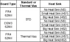
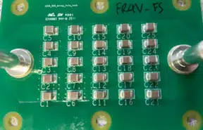
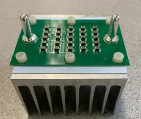
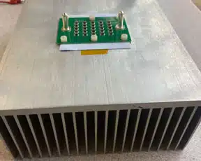
To expand on this concept, KEMET performed temperature rise measurements of a 5×5 array of C0G HV 1210 33nF 630V (C1210C333JBGACAUTO) using various thermal mitigation techniques as seen in Table 2. The purpose of this test was to show the impact of thermal mitigation techniques on the MLCC temperature rise under high AC conditions.
Tests were conducted on 2-layer FR4 and CEM3 substrates, with and without Thermal Vias, and with three heat sinking methods: No heat sink (NS), small heat sink (HS1), and a large heat sink (HS2). The NS condition places the PCB on top of a layer of FR4 for support without thermal interface material between the two.
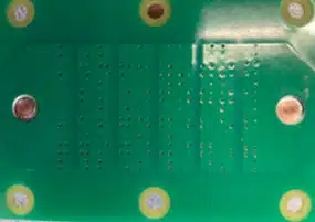
Figures 13 and 14 show the front and backside of the PCB with thermal vias. Both the bottom and top copper layers of the PCB are mirror images of each other.
Figures 15, 16, and 17 below show the three different heat sinking methods used for this test. When mounting the PCB to both head sinks, a thermal interface material was used between the PCB and heat sink.
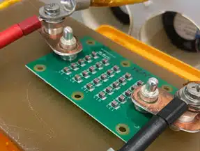
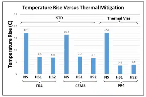
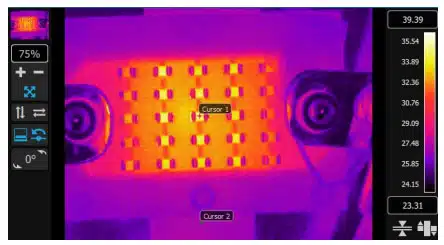
To simulate actual OBC conditions each configuration was tested under an AC voltage of 850Vrms at 85kHz while monitoring the temperature rise of the hottest MLCC. At 850Vrms, the total current through the array was approximately 15Arms. For each MLCC in the array, the AC voltage and current was 170Vrms and 3Arms respectively.
The results in Figure 18 show that the greatest temperature rise occurs when no heat sink was used regardless of board type or the use of thermal vias. At first, it would seem that the use of thermal vias with no heat sink would provide some thermal mitigation but it’s important to consider if the heat is able to be dissipated through the vias to a heat sink as shown in the 2R thermal models. In the case of the FR4 board with thermal vias and no heat sink, the total surface area of the backplane was relatively small and not thermally connected to a heat sink. This leads to a high MLCC to ambient thermal resistance causing greater temperature rise compared to the other solutions.
When utilizing a heat sink and no vias, the MLCC temperature rise was less than half of without a heat sink. This was not surprising since, even without thermal vias, the heat had a pathway through the thermal resistance of the PCB to ambient which was able to be more efficiently dissipated. When apply both a heat sink and thermal vias, the MLCC temperature rise was reduced even further now being roughly less than 4 times that of the PCBs with no thermal vias or heat sink.
CONCLUSION
The conclusions from this test are as follows:
- Using a heat sink with or without heat sink provides good heat dissipation.
- The use of a larger heat sink (HS2) versus the smaller heat sink (HS1) had negligible effects on the MLCC temperature rise.
- The combination of thermal vias and heat sinking provided the optimum heat dissipation and lowest MLCC temperature rise.
It must be stated that KEMET does recognize that using heat sinks such as the ones in the example are not practical in actual OBC applications. However, the purpose of the test was to stress the importance of dissipating heat generated by the I2R losses in the MLCC. During OBC power board designs, it is recommended to consider the self-heating of MLCCs under high AC conditions and how to dissipate heat generated under these conditions. Thermal vias can easily be adopted in the PCB design along with heat sinking methodologies that are within OBC design capabilities.
For example:
- Adding additional metal planes connected to the thermal vias.
- Separating the MLCC power board from the main power module and mounting it to any currently existing heat sinks or liquid cooled plates.
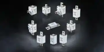
KEMET Solutions for Resonant Applications
C0G High Voltage: Datasheet
- Case Sizes: 1206 – 2225
- Voltage Range: 500V – 3000V
- Temperature Range: -55C – 125C
- Standard and Flexible Termination Options
KC-LINKTM: Datasheet
- For Fast Switching Semiconductors
- Case Sizes: 1812, 2220, 3640
- Voltage Range: 500V – 2000V
- Temperature Range: -55˚C – 150˚C
- Standard and Flexible Termination Options
KC-LINKTM with KONNEKTTM Technology: Datasheet
- High Density Packaging Technology
- Case Sizes: 1812, 2220, 3640
- Voltage Range: 500V – 2000V
- Temperature Range: -55˚C – 150˚C
Frequently Asked Questions about Resonant MLCC Capacitors for OBC Applications
apacitors in OBCs convert AC line voltages to DC voltage needed for charging EV batteries. They are crucial for resonance circuits (LLC topology), enabling high efficiency, miniaturization, and reliable high-frequency operation in EVs.
MLCCs offer miniaturization, superior high-frequency performance, and temperature/voltage stability, especially when Class 1 (C0G) ceramic is used. This makes them ideal for compact, efficient and reliable OBC designs.
Key factors include: temperature and voltage stability, ESR/dissipation factor, AC voltage and current capability, series-parallel configuration, and thermal mitigation (such as heat sinks with thermal vias to reduce temperature rise).
Use a series-parallel combination to reach the required AC voltage and current capacity. Validate actual self-heating and employ thermal mitigation, such as thermal vias and appropriate heat sinking on the PCB.
Class 1 (C0G) MLCCs deliver ultra-stable capacitance versus temperature and voltage with low ESR and dissipation factor, enabling high AC current handling and minimal self-heating. Class 2 (X7R) MLCCs are less stable and have higher losses.
How to Select and Implement MLCC Resonant Capacitors in OBC Applications
- Define Resonant Circuit Requirements
Specify the AC voltage, operating frequency, and required capacitance for your OBC LLC resonant topology.
- Select the Appropriate MLCC Class
Choose Class 1 (C0G) MLCCs for maximum stability and lowest losses. Avoid Class 2 (X7R) for critical resonant applications.
- Determine Series/Parallel Configuration
Use a series configuration to increase voltage rating and a parallel configuration to meet current and capacitance requirements.
- Verify AC Voltage and Current Capability
Ensure that the peak AC and RMS voltages do not exceed the MLCC’s rated DC voltage (guideline: Vpeak + VDC < Vrated, Vrms < Vrated/2√2). Confirm AC current will not cause excessive self-heating (<20°C rise).
- Implement Thermal Mitigation
Add thermal vias, connect MLCC pads to large copper planes, and attach to heat sinks as practical. Optimize PCB layout to direct heat away from MLCCs and reduce local thermal resistance.
- Validate in Real Application
Test at full AC voltage and expected frequency. Measure temperature rise and confirm the configuration meets both electrical and thermal requirements for long-term reliability.