
Atlas Magnetics, Co., “AM,” announces a high-performance magnetic material to reduce the size of the magnetic components used in consumer and IoT electronic circuits effectively removing the inductor from the PCB in applications such as DC/DC power conversion.
AM is a Nevada-based fabless semiconductor company focused on advance material deposition on standard semiconductor packaging film to create unique IC solutions.
AM solves the problem of direct integration of magnetics into integrated circuits “chips” by electroplating highly layered magnetic alloys directly on semiconductor epoxy packaging films for short connection to the semiconductor die using standard IC bumping processes.
This long-desired concept of using available semiconductor manufacturing processes to remove discrete components, such as inductors and transformers, was previously hindered by cost, frequency response, and incompatible processes. However, this development resolves these barriers while delivering the promised size reductions and performance enhancements by magnetic material deposition at temperatures and pressures compatible with semiconductor packaging.
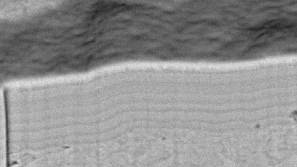
“While layering magnetic materials to create high frequency, high efficiency cores is nothing new, what’s new is how to cost effectively create micron to sub-micron layering. This is accomplished by reducing the process steps per layer from 13 to just 4. This simplified process allows new magnetic materials to be engineered for frequency (60 MHz or greater) and Qs (up to 35) with layering up to 60+ layers,” stated Atlas Magnetics CEO, John McDonald. “When these 0.2 to 0.4 mm cores are used in a finished inductor or transformer, values of up to 1 μH for lower power applications, and for high-power reduced inductance applications current densities of up to 10A/mm2 can be achieved.
In fact, the layering can be so fine as to yield materials with unique mechanical and electrical parameters. This opens new avenues of research for novel materials not previously economically feasible.”

