

This article based on Sotiris Zorbas, Power Εlectronics Εngineer Frenetic newsletter discusses optimisation of magnetic inductance for ZVS zero volt switching.
Our mission today is to understand how an LLC Converter achieves ZVS on the primary side.
The zero-voltage switching in an LLC Converter is directly linked to the magnetizing inductance of the Transformer and the output parasitic capacitance Coss of the mosfets that form the full/half driving bridge.
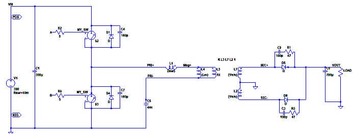
Let’s start from an LTspice schematic as you can see in Figure 1.
I have used a simple trick for the Transformer model: I kept the series and magnetizing inductances separate and used an ideal Transformer utilizing high inductance perfectly coupled inductors.
That way, I could monitor the magnetizing current going through Lm (L4) and that going to L3, thus the load eventually. L7, L2 secondaries are sized at 1H/n^2, where n is the turns ratio.
What else is important in that schematic?
Switches S2, S3 are working like on/off switches using the Rds_on of the selected mosfet each time. The important part is putting a couple of capacitors in parallel with these to model the output parasitic capacitance. That parameter can be found in the respective datasheets of the selected device. However, there is a trap here!
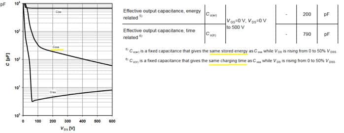
Is the output capacitance calculated based on time, or energy?
The output capacitance changes dynamically in mosfets when switching, ranging from a few picofarads to a few nanofarads, as the voltage on the drain-source pins drops from a high to a low potential. The manufacturer has constructed an artificial effective capacitor that either gives the same stored energy value or the same charging time.
Looking at Figure 2 helps to better understand what I’ve just described.
An example design – case study.
I have used the worked example in SLUA923 reference below, to help the reader. The specs are listed in Table 1.
The first thing when looking to achieve ZVS is to realize the working mechanism that causes the parasitic capacitances to be discharged. Without getting into many details, the resonant current in an LLC circulates through the LLC network and the power switches, causing ZVS of the latter. Part of the current is flowing through the magnetizing inductance Lm and part “flows” to the load through the ideal Transformer.
In Figure 3, the total current through the LLC tank marked as Itotal is L1’s current. Imag as the name suggests is Lm current. The difference of these currents flows into the ideal Transformer. Right at the switching transitions the Itotal equals Imag , and we can assume that this is practically constant during the transitions.
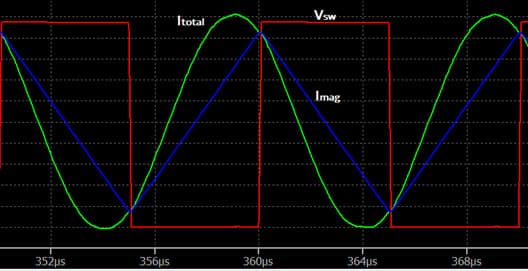
The rate of voltage rise dv/dt of the switching transition depends on the total capacitance to be charged/discharged (2*Coss_tr) and the actual peak current level, as shown in the figure 3. above. The usual 50-100ns of rise/fall times in 400V systems yields good results overall.
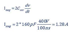
The magnetizing current swings triangularly from a maximum positive to a maximum negative value in T/2 as seen in Figure 3. At the moment of switching to get the 1.28A we just calculated, the current need to swing from -1.28A to +1.28A thus a ΔΙ=2Imag is the current swing.
Using the basic formula for an inductor:
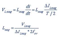
The voltage at the magnetizing Inductor is approximately half of the switching voltage because of the DC bias removal action of the resonant capacitor. So, in the end:
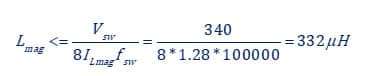
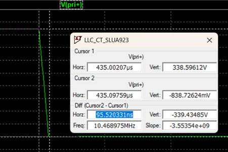
o achieve 100ns of switching time (0-100% of the voltage) we should select the magnetizing inductance below 332μH. Checking out LTspice in Figure 4 we can verify the correctness of the previous steps.
Conclusion
Proper selection of the magnetizing inductance ensures ZVS conditions over an extensive input voltage range. Of course, lowering the magnetizing inductance comes with the price tag. Reduced efficiency number at light loads (especially) is observed because of the increase in resonant current.

