
Dr. Mike Randall, Venkel LTd. has released whitepaper “The Definitive Guide to SMD Surface Mount Chip Resistor Selection” that assist with selection guide of SMD resistors.
Surface mount chip resistors are ubiquitous. Hundreds of billions of these devices are sold every year into myriad applications from handheld devices to precision lab test equipment to aerospace electronics and others.
Chip resistors and associated technologies are discussed from the standpoints of types, functionality, device design, and applications as well as circuit design and power rating considerations.
Careful consideration of these important factors should help lead you to the selection of the proper chip resistor component for your design.
Chapter 1: Background
Resistors impede current flow, causing a voltage drop when placed in an electrical circuit. Both alternating and direct currents are impeded by perfect resistors. The unit for resistance is Ohms (Ω), named after German physicist Georg Ohm. An Ohm is defined as the amount of resistance required to create a voltage drop of 1 volt (V), when the current flow is 1 Ampere (A). From a dimensional standpoint, an Ohm is defined as:

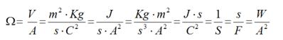
where:
- m is meter
- Kg is Kilograms is second
- C is Coulomb
- J is Joule
- S is Siemens
- F is Farad
- W is Watt
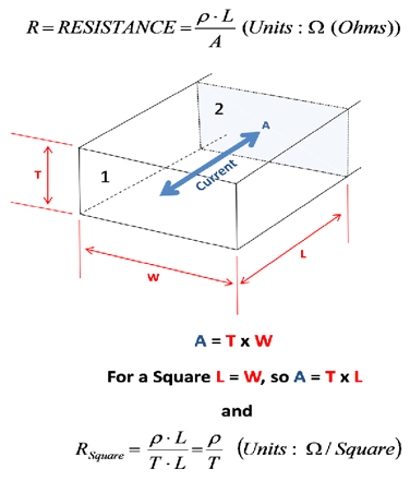
It is evident from the above that the Ohm may be described in many different terms including time, distance, mass, charge, energy, capacitance and power and conductance. As illustrated in Figure 1, the resistance to current flow between two planes (i.e., plane 1 and plane 2 in Figure 1) of cross sectional area within a conductor is found by the relation:

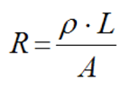
where:
- ρ is the resistivity of the material through which the current traverses (units, Ω-m)
- L is the length that the current traverses between planes 1 and 2 (units, m)
- A is the cross-sectional area of the conductor through which the current traverses (the area of either plane 1 or plane 2 (units, m2 )
This is bulk resistance, and the above relation can be further simplified if the conductor is broken into square segments (i.e., if W = L) as shown below. In that case, resistance simplifies to:

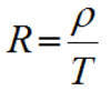
T is the thickness of the conductor through which the current traverses (units, m)
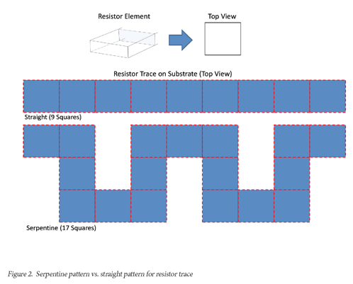
In the above case, resistance simplifies to a value having units of Ohms per square (Ω/h), which is typically called “sheet resistance.” Sheet resistance is a simplification of resistance that is useful to chip designers as it greatly simplifies the process of resistor design.
The chip resistor device designed will typically have at least one resistor element. The element is usually constant in thickness (T) with a geometry comprised of squares. The width and thickness of the trace helps establish power rating and the number of squares is utilized to determine the resistance of the device. Thus, it is important to maximize the number of squares in the design when it is desirable to maximize resistance within a small case size device. Thicker and wider squares typically result in the ability to carry more current and to handle more power, but the number of squares (and the resulting resistance per unit length) is reduced, limiting the maximum resistance possible within a given case size device.
During the chip resistor design process, the designer picks a material having a specific Ω/square value in order to enable the intended nominal resistance within the given package size. The designer will also utilize a serpentine pattern of interconnected squares in order to maximize resistance within the case size if needed, as a serpentine pattern of squares enables more resistance (i.e., squares) to be packed into a smaller area, thereby making the best of circuit board “real estate.” An example of this is illustrated in Figure 2. Use of a serpentine pattern of squares, in this case, enables almost 2X the resistance in the same lineal distance.

The resistor pattern is deposited onto a substrate, that is typically comprised of an alumina-based ceramic (typically Al2 O3 with from 1 w% to 10 w% glass as a sintering aid). However, other materials, such as silicon carbide (SiC), etc., may be used for high power applications or other application needs. The resistor patterns are typically deposited, many at a time onto a large substrate that is singulated into individual devices, later in the manufacturing process, in order to enable cost effective mass manufacture.
The resistor pattern is connected to two terminals that are also deposited on the substrate as well as around the edges of the substrate in order to form surface mount terminals, typically one on each end of the device, or in multiple stripes along the long sides of the device in the case of a resistor network. These exterior terminals or terminations enable connection of the chip resistor device with the circuit board. The resistor trace is trimmed to meet nominal resistance within the specification range for the device as necessary, and the resistor trace is over-coated with an electrically insulating material. After curing, the over-coat material is marked and each device is tested in order to create the finished chip resistor product which is then packaged (typically in tape and reel form) for storage, shipping, delivery, and placing or mounting with proper orientation.
During the circuit assembly process, the resistor device is then removed from the tape and is deposited on the circuit board (PCB) using a pick and place machine. Each chip resistor is then physically connected to the circuit within the PCB at the assembly facility using a thermal heat treatment that reflows solder in order to physically, thermally and electrically interconnect the resistor chip and the PCB. The solder is typically applied to the PCB prior to the chip placement operation by stencil printer deposition of specialized solder paste and the solder reflow process is typically performed in a carefully controlled reflow oven.
The resistor pattern is typically established via one of two methods, either thick film deposition or thin film deposition. Other, much less prominent methods of manufacture are used as well for certain application specific devices. As a result, chip resistors are typically categorized as either thick film chip resistors or thin film chip resistors based upon the deposition method used in their associated manufacture.
Thick film manufacturing processes usually involve the precision deposition of particle loaded liquids (e.g. inks or pastes) onto a substrate using some type of printing process (e.g., screen printing, stencil printing, pad printing or the like). The printed inks or pastes are then dried and fired to a dense, conductive, patterned resistor trace. Because patterning of the resistor is done during the application of the thick film ink or paste, this is called an additive process. Thick film resistor technology benefits from relatively easy composition modification as modification of the resistor thick film “ink” (e.g., chemistry, glass content, dopants for TCR, etc. for the resistor trace) is relatively easy to accomplish. Thick film resistor materials are generally based upon ruthenium oxide (RuO2 ) or platinum (Pt) mixed with specialized glass formulations and other dopants in order to achieved desired properties during firing.
The thin film chip resistor manufacturing processes typically involves the precision deposition of an un-patterned film or material onto a substrate. The deposited material is usually applied utilizing either thermal deposition in a relatively “hard” vacuum, or by physical vapor deposition using a sputtering process in a “softer” vacuum (e.g., a vacuum backfilled with Argon or other gas to increase the pressure) in order to create a plasma. Thin film deposition techniques usually result in very thin, uniform films. While thin films may be patterned during the deposition process, they usually are not when manufacturing chip resistors. After the precision deposition of the film, the film is typically patterned, post deposition, using photolithography. Because of this, the patterns are formed by removing material and the process is called a subtractive process.
Thin film resistor compositions are generally based upon vapor deposited nickel-chromium metals, called “nichrome.” This is generally done using physical vapor deposition via a sputtering technique. The resulting resistor elements generally need not be fired to achieve desired properties using this technique. It is relatively difficult to change the composition of the resistor element using thin film technology. However, thin film technology typically benefits from better deposit uniformity and more accurate patterning than thick film technology, so both manufacturing methods for chip resistors have their associated advantages and disadvantages.
The general resistor manufacturing process involves designing the device to achieve a specified range around the resistance nominal while maintaining the power rating in the package size of interest. Next, the resistor material is deposited onto the substrate, which is selected for mechanical strength as well as for electrical and thermal properties. The resistor element is patterned either during deposition (additive, thick film) or after deposition (subtractive, thin film), then adjusted to nominal resistance as needed, then over-coated and the individual resistor chips are singulated, then terminated, tested and packaged. In the case of thick film resistors, the resistor trace chemistry is carefully selected to set Ω/square as well as to adjust temperature coefficient of resistance (TCR) and other key properties, and the material is deposited and patterned in one step using screen or stencil printing (additive). The thick film resistor deposit is then thermal treated to achieve the electrical properties desired. In the case of thin film resistors, the resistor material is first deposited to achieve a highly uniform thin film, and is then patterned using photolithographic technics.
In the case of both technologies, the deposit thickness is carefully controlled to achieve the desired Ω/square, and the pattern is further adjusted, typically via LASER ablation, to achieve the desired resistance (nominal). The resistor pattern may also be adjusted for high voltage applications, or other specialized applications. The thickness and the pattern uniformity of thick film resistor elements is typically much thicker and less uniform for thick film resistors in comparison to thin film resistors, making thin film resistors more desirable for certain applications (e.g., those involving, precision tolerances, high frequencies, etc.).
Chapter 2: Resistor Types
Chip resistors come in many different resistor types, sizes, shapes and configurations. Thus, it is important to understand how each chip resistor will be used in your design. Before selecting your chip resistor device, it is prudent to be able to answers questions regarding your design needs, such as:
- What is the intended purpose and application environment?
- What values, tolerances, temperature stabilities and other specifics are required?
- What size can you accommodate and how much power will said resistor have to tolerate in its environment?
- What other environmental factors (e.g., RoHS, high sulfur atmosphere, or the like) are important to your application?
- Other questions depending upon your application and design constraints.
A Myriad of chip resistor types are available to address one’s design and application requirements such as:
- General purpose chip resistors
- High precision chip resistors
- Current sense chip resistors
- High voltage chip resistors
- High power chip resistors
- High resistance chip resistors
- Trimmable chip resistors
- Environmentally compliant and chemically stable chip resistors
General Purpose
General purpose chip resistors are used in surface mount circuit designs wherever a standard or general resistor such as for voltage reduction (voltage dividers), current control (current limiters), or the like is needed. These are typically thick film resistors, and are available in case sizes as small as 01005 (EIA). General purpose chip resistors exhibit temperature coefficient of resistance (TCR) values as low as +/-100 ppm/o C, with operating temperature range from -55o C to 150o C+, and have nominal values from as low as 0 Ω to 20 MΩ+, with power ratings ranging from ~0.01W to 2W+.
High Precision
High precision chip resistors are available in either thick film or thin film configurations. They typically exhibit very low change in resistance with changing temperature. The corresponding temperature coefficient of resistance (TCR) values for high precision chip resistors may be as low as +/-5 ppm/o C. Resistance tolerances are also very “tight” relative to standard chip resistors. For example ultra high precision chip resistors may have resistor value tolerances as tight as +/-0.01%. They are useful when it is difficult or impossible to trim or calibrate a circuit post assembly, or in other circumstances where tight tolerances and high levels of resistor value stability with changing temperature are required.
Current Sense
Current sensors are circuits that detect and convert current to voltage that is proportional to the amount of current traversing the circuit. Current sensing resistors are common for this purpose. They create a voltage drop when voltage is measured across the resistor. This voltage drop is directly related to the current via Ohm’s law (V=IR). The resistance is carefully selected so as to cause a voltage drop suitable to the circuit when passing currents in the range anticipated by the design. Current sense resistors are typically low value (<1 Ω) in order to avoid excessive power usage. Further current sense resistor information is available via Venkel’s Current Sense Resistors Cheat Sheet.
High Voltage
High voltage circuits are common for lighting, HV instrumentation, HV industrial or other HV applications. For these applications, it is likely that high voltage chip resistors are needed. These devices are designed to prevent arcing or voltage-related failure in circuits that are rated up to 3KV.
High Power
Applications requiring enhanced reliability or requiring high power density may benefit from the use of high power resistors in your design. High power resistors utilize special materials and designs to improve thermal properties in order to provide better power dissipation capability. High power resistors may be used in place of general purpose resistors where high power density is needed as they offer higher power ratings (generally a factor of at least 2 or more) compared to general purpose chip resistor analogs. They are well-suited for applications subjected to high current, or where a large de-rating margin is needed such as in high temperature environments or high power density applications or the like.
High Resistance
High resistance chip resistors are typically used in high impedance instruments, test equipment circuits, temperature measurement circuits, voltage dividers, circuits for gain setting, or other high impedance amplifier circuits or the like. High resistance chip resistors are typically thick film resistors ranging in case size from 0402 (EIA) to 2512 (EIA) or larger. Resistance values for these applications typically range from as low as 1 MΩ to 100GΩ+.
Trimmable Resistors
Some circuit designs require at least one tunable or trimmable resistor as it is very difficult to “design-in” the optimal value until all of the other variations within the circuit are accounted. Devices using circuits that require calibration such as certain Op Amps, oscillators, voltage dividers, tuned sensor circuits and the like may benefit from use of trimmable resistors. Trimmable resistors can be LASER trimmed, post mounting, to higher resistance than nominal as the resistor element and the glass passivation utilized are specially designed to allow in-situ LASER trimming after mounting the resistor to the circuit. This enables in-situ tuning of the circuit. In certain cases, trimmable resistors may even replace more costly and clumsy potentiometers as well.
Environmentally Compliant and Chemically Stable Chip Resistors
RoHS (restriction of hazardous substances) regulations have resulted in the reduction or elimination of lead, mercury, cadmium hexavalent chromium, brominated biphenyls and diphenyl ethers from electronic components and equipment, chip resistors included. In some cases, Pb is still allowed as a constituent (i.e., RoHS 5 or 5/6), but in many cases RoHS 6 or 6/6 is required. The demand for the latter is likely to increase in the future as environmental regulations and requirements further mature. The availability of chip resistors for application in high sulfur environments can be quite beneficial to device reliability as certain materials, such as silver or copper, tend to react with atmospheric sulfur, creating corrosion that can become a major reliability problem. Care in materials selection and resistor design can help avoid this problem.
Anti–sulfuration resistors increase the reliability of chip resistors in sulfuric or otherwise contaminated environments such as experiences with certain industrial atmospheres, or with in-tire electronics or the like, where reaction with sulfur at the resistor element-termination interface can result in increased resistance due to formation of silver sulfide at that interface.
This can occur with as little as 1-3 parts per million (ppm) sulfur concentration in the ambient. Anti-sulfuration resistors have been proven to prevent these types of failures.
Thus, as with other types of electronic components, it is critical to understand the temperature range and other environmental factors of your application as well as the voltages, power dissipations, resistance values, tolerances and other key requirements of the components that you select for your application
Chapter 3: Applications and Design Considerations
Power Considerations
The nature of resistors is to turn the flow of electricity into heat. They can dissipate considerable power as heat depending upon the design in which they are utilized. Resistors reduce voltage within a circuit, turning said voltage reduction into heat via Joule heating following the relation:


where:
- P = power (units, W)
- I = current (units, A)
- V = Voltage (units, V)
- R = Resistance (units, Ω)
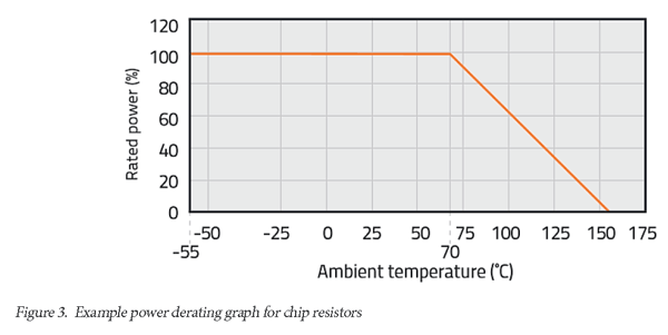
This creation of heat via resistive or Joule heating occurs within the resistor element of the device, causing it to heat up as it passes current. Some of the heat generated escapes from the resistor element to the outer environment, through the components of the chip resistor. Heat dissipation can only happen so fast however, and the amount of heat that is retained within the device heats it to higher temperature. The amount that the temperature increases is typically simplified to a linear value that is specified for the device. This value is typically stated in o C/W (units, degrees Celsius per Watt of power dissipated by the resistor element), and the nominal power rating of the chip resistor is determined from that value, amongst other considerations. The nominal power rating of a chip resistor is given in Watts. The value is determined by calculation based upon experimentation and is typically verified through reliability testing of several batches of qualification devices.
Further, the nominal power rating of the chip resistor decreases once the operating temperature of the device exceeds a given temperature (typically 70o C). In this case, the nominal power rating of the chip resistor is reduced at a rate of ~-1.2%/o C as the device temperature increases past 70o C, as indicated in the illustration below, and the chip resistor is completely derated by 155o C (the maximum use temperature). It may also be possible to increase the rating of the chip resistor selected if the operating temperature of the chip resistor is always kept below 70o C using an extrapolation of the derating line in Figure 3 to temperatures less than 70o C (e.g., ~+1.2%/o C below 70o C), but be sure to get your supplier’s “blessing” before you do this, as this practice may result in warranty issues regardless of whether or not it is appropriate.
Improper chip resistor selection with respect to power rating may result in aging (embrittlement) or even melting of solder joints, which will lead to a lack of reliability of the chip’s solder joints. It can also result in a loss in printed circuit board (PCB) performance, or even failure of the PCB. Improper component selection or circuit design can also result in poor chip resistor performance, such as high drift in resistance value, or the like. These effects may not be reversible without reworking or even replacing the component.

For proper design, the circuit designer needs to carefully consider the balance between component selection and thermal management considerations in order to achieve a thermal equilibrium condition in the device that does not significantly exceed the operating temperature of the circuit. Heat generated during operation must be removed from the device in an efficient manner. Heat may be removed via one or more of the mechanisms of conduction, convection or radiation. However, in this case, radiation and convection are typically only minor contributors to heat flux as the temperature is too low to emit significant radiation, and the ambient around the chip resistor device is typically a poor convective medium. So we must rely on conduction for removal of the large majority of the heat generated from a chip resistor in its associated circuit.
The primary path for removal of the heat generated is the conduction path of heat through the metal terminals of the chip resistor, to the conductive traces of the PCB and out into the thermal mass of the PCB. This heat flow can be maximized in the design of the chip resistor by maximizing the size of the terminals (i.e., using a large case size chip resistor) or through the use of larger solder connections, or through the use of two sided metallization and/or thicker metallization on the PCB, or the use of prudently placed thermal vias in the vicinity of the mounting pads. Each of these methods, especially when used in combination, results in an improved thermal conduction path for heat from the chip resistor.
Further, material selection is important. For example, the thermal conductivity (symbol, KTh, units, Watts per meter degree Kelvin, W/mK) of alumina, the material typically used for chip resistor substrates, is ~24-30 W/mK. Use of more exotic electrically insulating materials for the chip resistor substrate, such as Silicon Carbide (SiC, KTh ~350- 500 W/mK) or even diamond (C, KTh ~900-3,000 W/mK), helps to increase the power rating of the device by providing a greater dissipation path for heat generated in the resistor element. However, use of these materials can be highly expensive, and it is important to balance the improvement in thermal performance with the cost of utilizing exotic materials. In the case of diamond, for instance, the increase in cost is usually prohibitive. The above discussion also applies to the over-coating material and to the terminal materials.
Additionally, thermally conducting, but electrically insulating materials, such as thermally conductive epoxies or the like, may be used to underfill the chip resistor in order to enhance thermal conduction from the bottom of the chip resistor into the PCB. Thermal vias below said underfill can further enhance conduction of heat from the chip resistor to the PCB as well.
Applications

Resistors are used in numerous applications, such as current sensing, circuit tuning, voltage dividing, gain setting, high frequency terminations and myriad high voltage and high power applications. Many of these applications may also be environmentally challenging, such as high temperature, high sulfur or high humidity atmospheres or the like. Thus, it is important to understand the potential effects of precision/matching, frequency, temperature and current in your design as each may be an important factor in your application.
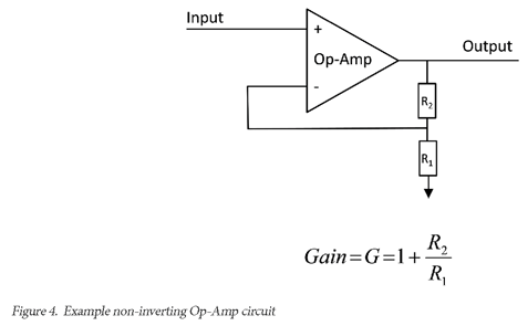
In certain applications, it is highly important to use resistors that are well-matched. For example in the non-inverting amplifier circuit (Op-Amp based) illustrated in Figure 4, the gain (G) is established by the ratio of the resistor values shown through the relation G = 1 + (R2 /R1 ). If a minimum amplifier precision of 1% is required, then the nominal resistance values of resistors R1 and R2 could give as much as ~0.5% maximum error. Further, it is important that the resistors used in this application have well-matched temperature coefficient of resistance (TCR).
For example, using resistors having TCR of 200 ppm/o C would result in 1% change in gain (G) if Δ temperature (ΔT) between them is 50o C. This could occur as a result of self heating of R2 for instance, or if one of the resistors is placed too close to a heat source (e.g., high power actives or the like). For high precision systems (say 10 bit, requiring 0.1% G accuracy or better), matching of R1 and R2 , combined with use of low TCR (and similar TCR) resistor materials becomes important. Additionally, design that minimizes ΔT between R1 and R2 is important. In these cases, the use of high precision resistors or of matched resistor networks is a common solution. Trimmable resistors may also be valuable in these applications.
Temperature effects are not only important for resistors that must be matched, but are also important in other applications requiring stable resistance. Low TCR is generally preferred, but must be balanced with the economic factors of your design, as low TCR resistors are generally more expensive. The effect of TCR on resistance is calculated using the relation:

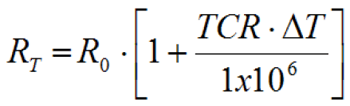
where:
- RT is resistance at the temperature of interest (Ω)
- R0 is the nominal resistance (Ω)
- TCR is temperature coefficient of resistance (PPM/oC)
- ΔT is the change in temperature from nominal (oC)
Indicating that the use of low TCR materials in the resistors that are used in your design is preferred, and that ΔT in your circuit’s operating environment should be kept to a minimum in order to avoid resistance changes in your design.
Additional variation in resistance may result from thermoelectric effects. Chip resistors typically are made from at least two different conductor materials; the resistive element is generally one material and the external terminal material, or the termination, is generally at least one different conductor material. When dissimilar metals are joined, a thermocouple may be formed due to the Seebeck effect. This effect results in the generation of a small voltage between the terminals of the resistor that is based upon the difference in temperature (T) between the terminals. It is similar to the phenomenon that results in a thermocouple output voltage that makes thermocouples useful for measuring temperature. This effect can be significant in precision circuits, so it is important to design your circuit such that ΔT between each chip resistor terminal is minimized (e.g., design such that cooling airflow traverses each resistor terminal equally, or design that avoids placement of one terminal near a heat source, or the like).
Random thermal movement of charge carriers in a resistor element also produces noise that is proportional to the operating temperature, as well as to the use bandwidth, the current and the resistance of the device in a one half power manner. This can become significant as one or more of operating temperature, current, use bandwidth or resistance is increased.
Frequency Considerations
While a resistor is conceptually simple, each has non-ideal characteristics, as no device is perfect. In the case of a chip resistor, said device will have capacitive and inductive parasitics. The effect of the capacitance can be modeled as a capacitor in parallel with the resistor, and the effect of inductance as an inductor in series with the resistor. Parasitic capacitance of chip resistors tends to be quite small (e.g. <10pF), leading to low frequency (near DC) impedance that is generally >100GΩ, which will have minimal effect on the resistnace value of all but the highest resistance value resistors. This effect is generally compensated during the desgin process but should be understood as the compensation likely changes with frequency. With increasing frequency the impedance associated with the parasitic capacitance is reduced. This effect can be significant when capacitive impedance is similar to, or less than, the nominal resistance value. For example, in the case of a parasitic capacitance of 1.6pF, the associated capacitive impedance at 100GHz will be about 100Ω. This parasitic could affect the actual impedance by as much as 33% in the case of a 50Ω termination resistor at 100GHz.
Again, this is usually compensated in the design, but it is important to understand as the effect changes with frequency and with resistance value. The inductive parasitic may also be important at high frequencies. For example, a parasitic inductance as low as 10 nH at 100 MHz will contribute about 50 Ω in to the impedance of the resistor. Again, this is compensated for during the design process in order to achieve proper performance over a range of frequencies, and thus is important to the understanding of the frequency range appropriate to the device selected for your circuit and your situation, as the combined effect of the parasitics upon overall impedance changes with changing frequency.
Also, as frequency is increased in an AC circuit, current flows more and more toward the periphery of the conductor through which it flows. This is called the skin effect, and may result in increased impedance as frequency is increased. The current density in a conductor (or resistor element) decreases from the outside to the inside of the conductor according to the relation:

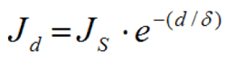
where:
- Jd is the current density at depth d into the conductor (units, A/m2 )
- JS is the current density at the surface (s) of the conductor (units, A/m2 )
- d is the depth into the conductor (units, m)
- δ is the skin depth of the material comprising the conductor (units, m) as defined by the relation:

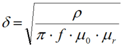
,where:
- ρ is the resistivity of the conductor or resistor material (units, Ω-m)
- f is frequency (units, Hz)
- µ0 is the magnetic permeability of free space (units, 1.257×10⁻⁶ H/m)
- µr is the magnetic permeability of the conductor or resistor material (units, H/m)
Skin depth is the depth into a conductor at which the effective conductivity of a material is reduced to 1/e (~37%) of its full value at the exterior skin. As frequency and/or magnetic permeability are increased, skin depth δ decreases at a half power rate, and as resistivity increases, δ increases at a half power (square root) rate. This is important mainly in thick film resistors where the thickness of the resistor element(s) tends to be considerably greater than for thin film analogs, making thick film resistors generally more susceptible to increased impedance at high frequency, as compared to thin film resistors, due to the skin effect. Additionally, perimeter geometries of printed thick film resistor traces tend to be less consistent compared to thin film resistor traces, and as the current is forced toward the outer portion of the conductor, the current path becomes more tortuous, further increasing apparent impedance at elevated frequencies in thick film resistors. Magnetic permeabilities and resistivities of the resistor trace materials are also important considerations. To minimize the skin effect (i.e., to maximize δ), it is generally preferable to use high resistivity, low magnetic permeability materials, and to understand these values at the frequencies and fields of your application as they may change greatly with changing field or frequency.
Chapter 4: Summary of SMD Chip Resistors Selection Guide
Resistors have a myriad of applications in electronic circuits. It is important to understand the operating parameters required for your design when selecting a chip resistor. For example, it is important to consider power rating when selecting a chip resistor, and while it may be tempting to use the smallest chip resistor possible, that may not be prudent as it may lead to overheating and associated reliability issues. As the balance between heat generation and heat dissipation is paramount, it is important to select the appropriate chip resistor as well as to properly design your PCB, making sure to use the appropriate amount of metal in the traces and lands, as well as thermal vias, etc. where prudent. The balance between power dissipation and cost is an important consideration as well, since use of high thermal conductivity materials and specialized designs and cooling schemes, etc. can quickly become prohibitively expensive.
For gain setting applications, it is important to make sure that precision and TCR are appropriate. Use of a resistor network, or precision resistors, or trimmable resistors may be most appropriate. In order to avoid temperaturerelated resistance change, as well as other signal noise related effects, it is important to design for minimal ΔT both between resistor terminals and between individual resistors in your circuit, as well as to keep the overall temperature of the resistors as low as practicable. It is also important to understand how parasitics affect resistor performance as frequency is changed, and to minimize parasitics in a manner that is cost effective for your application through both device selection and circuit design. For high frequency applications, skin effect may become important, and the potential geometric advantages of thin film resistors over thick film resistors, as well as the properties of the resistor materials used in the device selected, should be carefully considered.
High power chip resistors are designed using high thermal conductivity materials, combined with resistor patterns having better thermal properties, and by utilizing modified construction and processing techniques, all in a cost effective manner. High power chip resistors may have double the power rating, or better, compared to the same case size standard chip resistor. Because of this, they are typically an economic option for the designer when it is important to maximize power density as well as component density within the circuit design. Additionally, if the designed circuit is kept below 70o C, it may be possible to increase the power rating of a chip resistor using a slope similar to, or less than the slope of the derating line extrapolated to the operating temperature below 70o C. Be sure to talk to your chip resistor supplier, prior to adopting this practice, in order to make sure that this practice does not void any warranties, however.
original paper and pdf download is available at the link below

