


This article provides comparison benchmark of gallium nitride vs silicon semiconductors in soft switching LLC power supply applications with evaluation using different LLC transformers. The article was written by Jakub Jirsa – STMicroelectronics, Power Application Engineer and Octavian-Tudor Stroe – Würth Elektronik, Product Definition Engineer.
Gallium Nitride (GaN) is a wide bandgap compound semiconductor formed by the combination of Gallium and Nitrogen with an atomic structure of wurtzite crystal. Due to its 3.4 eV (electron*Volt) band gap it can be used in optoelectronics (blue LEDs and violet laser diodes), high-power and high-frequency devices.
Since early 2020, there has been seen an increasing use of GaN power transistors in power supplies. Capable of high breakdown strength, fast switching frequencies, high thermal conductivity and very low on-resistance, devices that are based on GaN show increasing performance compared to Silicon (Si) based devices. All these parameters translate into increased efficiency and components size shrinkage, therefore reducing the cost of many power conversion systems and final products.
In contrast to Silicon Carbide (SiC) power devices that have been around for quite a while, GaN power devices have just started to appear on the market. GaN offers many of the performance benefits of SiC with the prospect of accrued competitiveness because it is grown on a larger, lower-cost Si substrate and can be produced in renovated CMOS fabs. However, the technologies used in SiC and GaN power switches are quite dissimilar. The SiC for instance is a harder material and requires more sophisticated manufacturing techniques at far higher temperatures with respect to silicon; annealing is done at 1700 °C and ion implantation at 500 °C vs. 800 °C and 25 °C, respectively.
GaN switches, on the other hand, are derived from RF HEMT (high electron-mobility transistors) technology, which differs from that of the silicon power FET. A summary of parameters for each technology can be seen in Table 1 below.
| Parameter | Si | SiC-4H | GaN |
|---|---|---|---|
| Bandgap (eV) | 1.1 | 3.2 | 3.4 |
| Electron mobility µn (cm²/V s) | 1450 | 900 | 2000 |
| Breakdown Electric Field Ebr (MV/cm) | 0.3 | 3 | 3.5 |
| Saturation electron drift velocity VS (107 cm/sec) | 1 | 2.2 | 2.5 |
| Thermal conductivity Q (W/cm K) | 1.5 | 3.8 | 1.3 |
SiC MOSFETs and GaN HEMTs are largely complementary as each one of them addresses different applications. Electric Vehicles are benefiting from large-scale adoption of both, with SiC MOSFETs and their ability to operate at voltages between 650V and 2200V, being ideal for traction inverters, DC-DC converters and on-board chargers (OBC).
Operating at voltages from 650V down to 100V, GaN may eventually also be a valuable technology for the latter two applications, due to its higher frequency capability, as it becomes more mature and cost effective.
As a key supplier of power solutions, STMicroelectronics has heightened efforts to complement its offer with wide bandgap materials (WBG) such as Silicon Carbide and Gallium Nitride.
The MASTERGAN series is an advanced power system-in-package integrating a gate driver and two enhancement mode GaN transistors in half‑bridge configuration. It features UVLO protection on both the lower and upper driving sections, preventing the power switches from operating in low efficiency or dangerous conditions, and the interlocking function avoids cross-conduction conditions. The input pins extended range allows easy interfacing with microcontrollers and DSP units. The series operates in the industrial temperature range, -40°C to 125°C. The devices are available in compact 9 x 9 mm QFN packages.
STMicroelectrinics’ MasterGaN platform includes MasterGaN1, MasterGaN2, MasterGaN3, MasterGaN4 and MasterGaN5 available with different RDSon of GaN transistor (Static drain-source on-resistance), to better address specific application requirements. To help developers evaluate the characteristics of MasterGaN platform and to quickly create new topologies without the need of complete PCB design, a demonstration board is available for each MasterGaN device. Table 2 below shows the typical applications suited for each of the MasterGaN families.
| Solution | Application |
|---|---|
| MasterGaN1 | OLED TV, LED lighting, Adapter, Telecom/Server power, Power supply for 5G |
| MasterGaN2 | Fast & wireless charger, AC-DC adapters USB-PD |
| MasterGaN3 | Fast & wireless charger, AC-DC adapters USB-PD |
| MasterGaN4 | LED lighting, Power for PC, Power supply for 5G |
| MasterGaN5 | AC-DC adapters USB-PD, LED lighting |
Based on Table 1, wide electron mobility and wide band-gap materials are already objective indications of the superior performance of the GaN based device in certain applications. However, to see the benefits in real application, there are other important electrical parameters that are worth exploring. For example, GaN transistors have a much lower gate charge. To charge the intrinsic capacitances of the gate generates losses in the gate driver, gate turn on/off resistors and the internal structure of transistor. These losses are given by Equation 1:
PGateCharge = fSW * VCC * QG
, where
- fsw is switching frequency of the converter
- VCC is supply voltage of gate driver
- QG is gate charge needed to charge input capacitance of transistor
Since the input capacitance is non-linear, the gate charge curve can be found in every datasheet. Figure 1 shows a comparison of the gate charges for the corresponding transistor in SiC, Si and GaN MOSFET technology and already reveals an indication of superior performance of GaN technology in high frequency applications with lower gate power losses.
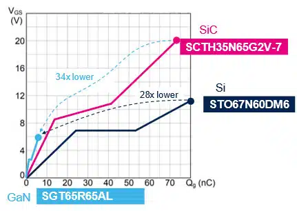
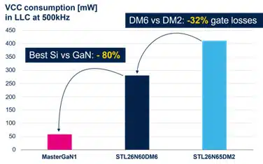
Figure 2 compares the losses caused by the gate charge from a real application. It shows the measured power loss (the VCC consumption) of the gate driver IC in an LLC topology, switching at 500kHz. The comparison is made between 2 different Si MOSFET generations, DM6 and DM2, and the GaN based module MasterGaN1. Significant improvements were brought to the Si based transistor in last super-junction generations that reduce gate losses by 32% but comparing the best Si MOSFET at the time of comparison to the MasterGaN1, an immediate huge difference of 80% can be noted in the reduction of gate power losses. Clearly, the high switching frequency is better suited for a GaN application in this case.
Just measuring the power consumption of the gate driving IC under the same operating conditions is one way to directly understand the benefits of GaN over Si based MOSFETS. Another way to understand it from a more scientific perspective is to look at the same designs with an oscilloscope probe and measure the resonant transient in the LLC topology. A lower parasitic output capacitance allows for faster charge of the transistor and tighter control due to lower rise times. The transient measurements below (Figure 3) prove this by showing an almost 4 times shorter dead-time for the GaN compared to equivalent superjunction MOSFETs. The results were obtained using an existing reference design for a 250W LLC power supply, 400 Vin and 12 Vout.
On paper the differences are obvious with clear advantages on the GaN side compared to Si based devices, but is there any difference when it comes to application type? Or power topology? There are many factors to consider when choosing one technology over the other, like the final application, power topology used for the converter and the passive elements around the switching converter.
So, is it useful to select GaN if the design requirement is 100kHz switching frequency, resonant topology and there is no need for a high-density?
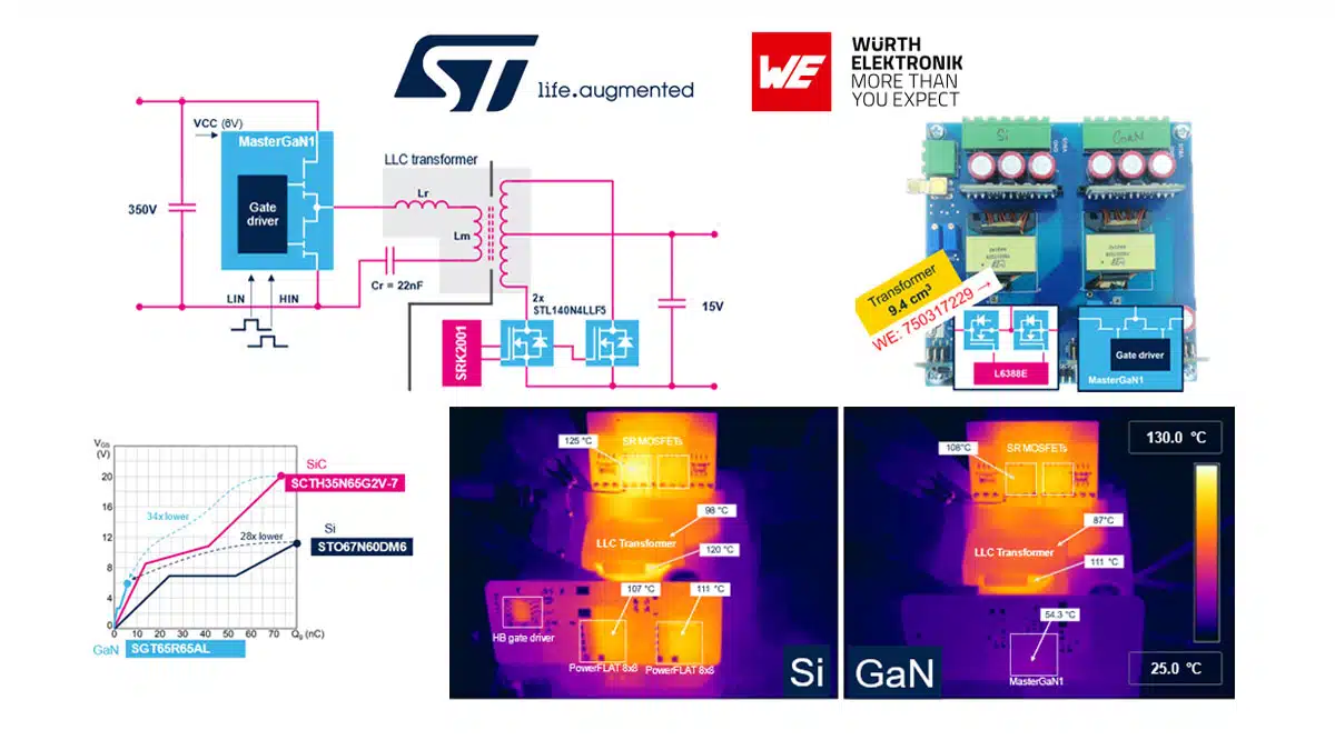
To answer this as effectively as possible a direct comparison had to be made with a real application. Here, Wurth Elektronik, as a passive components manufacturer joined forces with our valued partners, STMicroelectronics, in a small research project to consider this topic. For this, two LLC power supplies were chosen for analysis. First, a 250W, 350V to 15V converter with a convenient switching frequency of ~110 kHz and second a 200W, 350V to 15V converter with a higher operating frequency of 370 kHz, were chosen. 2 different LLC transformers were used to further evaluate the differences, specifically designed for this performance benchmark. Before we go to the test results let’s have a quick look at an LLC topology and test setup.
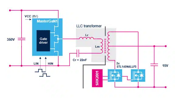
Figure 4 below shows a simplified schematic of LLC power topology used for the tests. In the center of the figure, there are 3 elements at the heart of the circuit: the resonant tank formed by the resonant inductor – Lr, the magnetizing inductor – Lm and resonant capacitor – Cr. The resonant inductor is usually integrated into LLC transformer established by leakage inductance.
Further efficiency tests were conducted for an output power of 150W, 200W and 250W, with GaN and Si based (Figure 5), first with a comparison of efficiency at a low switching frequency of 110 kHz and an off-the-shelf standard transformer and then for 370 kHz frequency with a much smaller transformer optimized for the increased operating frequency. A summary and overview of the boards and results are shown below.
| Technology | Si | GaN | Si | GaN |
|---|---|---|---|---|
| Frequency | 110 kHz | 370 kHz | ||
| Power Output | 150 W | |||
| Efficiency | 92.4 % | 92.8 % | 88.4 % | 92.4 % |
| Power Output | 200 W | |||
| Efficiency | 95.8 % | 96.3 % | 92.5 % | 94.5 % |
| Power Output | 250 W | |||
| Efficiency | 95.02 % | 95.75 % | N/A | |
The test shows that for a low switching frequency, as expected from the theory, there is no relevant difference between Si and GaN based devices. On the other hand, increasing the frequency, which in turn also allows us to decrease the size and the inductance of the transformer, resulted in a 4% increase in efficiency by using GaN at 150W.
At 200W output, the GaN still achieves a higher efficiency with a higher switching frequency compared to Si, even if it is just a 2% increase. At lower switching frequencies, the difference between Si and GaN is small for every power output.
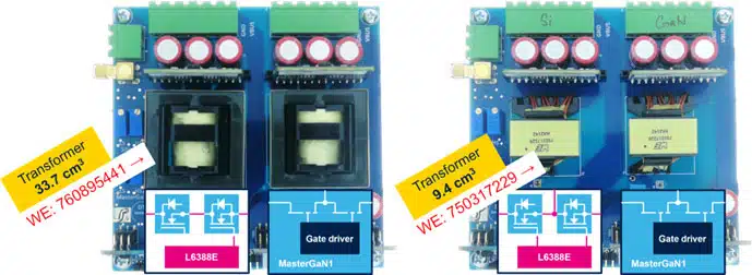
An advantage of using a higher switching frequency can be noted in the size of the transformer, which in turn translates to decreased losses in the transformer as well, not just for the MOSFET or the gate driving IC. The volume ratio between the two transformers is 1:3.5 and the difference can be clearly seen in the side view from Figure 6.
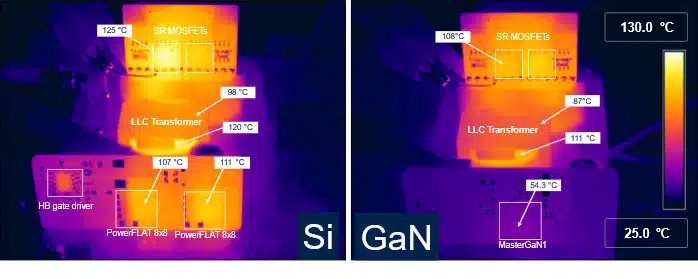
Figure 7 below shows IR measurements at different points on the evaluation boards running at 370kHz switching and 200W output power. Moreover, a small size means a smaller PCB or the possibility of high-density designs further optimizing costs.
The LLC topology can be used in a wide variety of power levels which in turn influence factors like EMC input filter, output filtering capacitor and the use of an external resonant inductor or the transformer built with an integrated resonant inductor by using the leakage inductance. All of these topics are covered by Wurth Elektronik’s extensive portfolio, ranging from EMC solutions, inductors and capacitors to custom designed magnetics capabilities. A wide variety of solutions for the EMI filtering are possible, ranging from the use of common mode chokes with NiZn, MgZn, NiZn + MgZn or Nanocrystalline core materials for a variety of attenuation factors over a broad frequency range, to the use of ferrite beads, filter chokes and hybrid polymer capacitors. The WE-HCFT with either flat wire or round wire is an excellent candidate for the external resonant inductor in the LLC topology, or if a litz wire for low AC losses is necessary then one can choose from the WE-HCF series. Further improvements to the off-the-shelf parts can be made depending on the requirements through the custom magnetic service we offer.
With increasing power, the necessity of isolated drivers becomes more important to ensure efficient and robust driving of GaN devices (or even SiC). For the isolated driving ST offer galvanically isolated gate drivers family called STGAP. To properly operate these gate drivers, the isolated auxiliary supply is needed. Wurth Elektronik developed a new series of auxiliary gate supply transformers, the WE-AGDT series, offering ultra-low interwinding capacitance ideally suited to keep the parasitic capacitance barrier as low as possible in order to maximize common-mode transient immunity and keep the noise from coupling from high voltage side to low voltage side. Combined with ST’s synchronous iso-buck converter – L6986I or latest L6983I offer excellent solution to drive GaN or SiC transistors.
Conclusion
The new GaN technology allows us to achieve soft switching converters at higher switching frequencies. There are two reasons why the higher frequencies are possible: lower gate charge and smaller parasitic output capacitance of GaN transistors.
With an increase in switching frequency the designer has the advantage of a reduced board area by reducing the size of the main transformer, which allows the engineer to design higher power densities in the same area compared to Si based devices. However, the lower input capacitance of GaN transistors tends to be sensitive to any noise and more care must be given to the layout around the main switching loop due to the higher switching speeds.
On the other hand, looking at the direct comparison between Si and GaN, at lower switching frequencies, we notice that there is no real benefit in using GaN for now. This would only increase the costs resulting in a poor ratio of efficiency vs. cost. If high switching speeds and high-power density are not the main requirements, it is still better to go with a Si based device.
Moreover, why bother with the EMI issues associated with high switching speeds if not necessary? Nevertheless, STMicroelectronics and Wurth Elektronik are here to provide you with a complete solution from both active and passive side with experts ready to support your implementation of GaN devices with the best transformers and inductors to squeeze the last ounce of efficiency out of the design.