
Bogdan Adamczyk and Dimitri Häring from the EMC Center at Grand Valley State University, USA discuss the second- and third-order low-pass EMC filters in article published by InCompliance Magazine.
First, the insertion loss a general filter is defined, and then the impact of the source and load impedance on the insertion loss is investigated. Simulations and measurements focus on the CL and LC filters. In Part II (to appear in the next issue) the performance of the Pi and T filters is evaluated and compared to that of the CL and LC filters.
Insertion Loss and Basic EMC Filter Configurations
EMC / EMI filters are described in terms of the insertion loss defined as [1],


where VL is the magnitude of the complex voltage L. Figure 1 illustrates this definition.

Since VL, without filter > VL, with filter the insertion loss defined by Eq. (1a) is a positive number in dB. The insertion loss could alternatively be defined as

In this case the insertion loss in dB is the negative of the loss defined in Eq. (1 b). We will use this definition when plotting the simulation results, and comparing the simulation results to the VNA measurements.
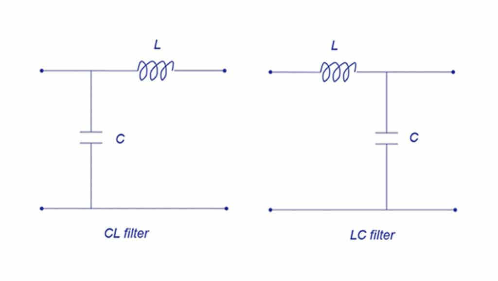
A typical 2nd -order EMC low-pass filter consists of a series inductance and shunt capacitance [2]. Figure 2 shows two different filter configurations.

3rd-order π and T filters are shown in Figure 3.

Source and Load Impedance Effect
Note that for each order of the filter we have two different configurations. Which one will perform better, i.e., which configuration has the larger insertion loss (in the negative sense)? As we shall see, in most cases, this depends on the impedance of the source and the load.
The general rule is that the inductor should be on the low-impedance side and the capacitor should be on the high-impedance side [2, 3].
Thus, when both the source and the load impedances are low, the appropriate configuration from the ones shown above is the T filter, shown in Figure 4. When both the source and the load impedances are high, the appropriate configuration is a π filter shown in Figure 5.
Figure 6 shows the appropriate configurations when the source impedance is low and the load impedance is high. Finally, Figure 7 shows the appropriate configurations when the source impedance is high and the load impedance is low.


Verification via Simulations and Measurements (CL and LC filters)
Let’s verify some of the above claims by investigating the second order CL and LC filters. First, let’s focus on the configurations shown in Figure 6, where the source impedance is low and the load impedance is high.
Figure 8 shows the LT spice simulation schematic. The 50 Ohm source impedance is provided by the network analyzer at Port 1. The measurement made by the network analyzer at Port 2 is across its internal 50 Ohm impedance. This is shown in Figure 8(a). To vary the impedance at the source or the load, an in-line resistance could be inserted at either or both sides. Figures 8(b) and (c) show the configuration where 1kΩ impedance is inserted on the load side.

Figure 9 shows the insertion loss (according to Eq. (1b)) of the two filter configurations.

As can be seen from Figure 9, the LC filter clearly outperforms the CL filter. The insertion loss of the LC filter at 10 MHz is about 15 dB higher than that of the CL filter. This is consistent with the general rule that the inductor should be placed on the low-impedance side and the capacitor on the high-impedance side.
To verify the simulations results the measurement setup shown in Figure 10 was used.


Since a four-channel network analyzer was used, we could evaluate the two different filter configurations simultaneously. Figure 11 shows a close-up of a PCB filter board used in the measurements.
Figure 12 shows the measurement results for the two configurations shown in Figure 8 and simulated in Figure 9.

Clearly, the LC filter outperforms the CL filter, which is consistent with the simulation results. In the frequency range 100kHz – 10 MHz the simulated and measured results are remarkably close, as summarized in Tables 1 and 2.
| CL Filter | f = 100 kHz | f = 1 MHz | f = 10 MHz |
| Simulated Insertion Loss | 21.2 dB | 30.8 dB | 50.7 dB |
| Measured Insertion Loss | 21.3 dB | 30 dB | 49 dB |
Table 1: Simulated and measured insertion loss for CL filter
| LC Filter | f = 100 kHz | f = 1 MHz | f = 10 MHz |
| Simulated Insertion Loss | 21.2 dB | 30.8 dB | 65.8 dB |
| Measured Insertion Loss | 21.3 dB | 30 dB | 65.7 dB |
Table 2: Simulated and measured insertion loss for LC filter
At 10 MHz the difference between the simulated insertion losses of the two filters is 15.1 dB which is close to the measured difference of 16.7 dB.
The measured results show the self-resonant frequency at 30 MHz, with the insertion loss of 84.9 dB for the CL filter and 115 dB for the LC filter. A second resonance occurs at 60 MHz with the insertion loss of 83 dB for the CL filter and 95.5 dB for the LC filter. These resonances were not predicted by the simulation models, as those models assumed ideal components and did not account for the board parasitics.
The measured results clearly show that, ver the entire frequency range, the LC filter (inductor on the low impedance side and capacitor on the high impedance side) has a higher insertion loss than the CL filter (capacitor on the low impedance side and inductor on the high impedance side).
References
- Clayton R. Paul, Introduction to Electromagnetic Compatibility, Wiley, 2006.
- Bogdan Adamczyk, Foundations of Electromagnetic Compatibility with Practical Applications, Wiley, 2017.
- https://link.springer.com/content/pdf/10.1007%2F978-3-642-27326-1_90.pdf
Dr. Bogdan Adamczyk is professor and director of the EMC Center at Grand Valley State University (http://www.gvsu.edu/emccenter/) where he develops EMC educational material and teaches EMC certificate courses for industry. He is an iNARTE certified EMC Master Design Engineer. Prof. Adamczyk is the author of the textbook “Foundations of Electromagnetic Compatibility with Practical Applications” (Wiley, 2017).
Dimitri Häring received his Master’s Degree in Electrical and Computer Engineering at Grand Valley State University in 2019 where he worked with Prof. Adamczyk at the EMC Center. Currently he works as an RF design engineer. His further interests are Internet of Things and Embedded Systems programming.

