
Source: Electronic Products, Signal Transformer article
Understanding the basics of the switch-mode converter principle will help designers select the best inductor for their application. By Mitchell Rhine, director of engineering, Signal Transformer.
Traditional linear voltage regulators have one major drawback: The voltage dropped across the pass transistor multiplied by the load current equals wasted power. The preferred option is often a switch-mode DC/DC converter, wherein the power transistors are continuously switching with a duty cycle that, with some additional filtering, delivers the required output voltage.
In this configuration, the transistor is either ON, involving no voltage drop, or OFF with no current passing. This means that the power dissipation tends to go down to zero when switching between states, yielding an efficiency of up to 95%, while linear converters typically deliver about 50%. Switching converters have another major advantage in that their topology means that they can operate in step-down (so-called “buck,”), step-up (“boost”), or invert (“buck-boost”) modes.
A basic understanding of the switch-mode converter principle is helpful in selecting the inductor required. This article will focus on just a few basic configurations, primarily on the very popular fixed-frequency buck converter operated in “continuous mode.”
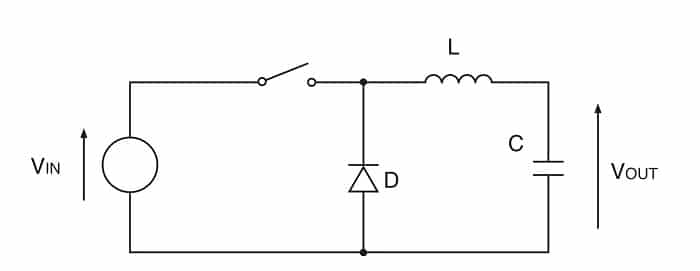

Fig. 1: A simple switching DC/DC converter.
A basic buck converter consists of just a switch, inductor, capacitor, and diode (Fig. 1). Assuming an ideal switch and diode, Vsw = 0 and Vd = 0, simplifies the explanation of the converter’s operation. In a real-world design case, to accurately determine the required inductance value L, the expected duty cycle D, and operating efficiency, Vsw and Vd have to be considered non-zero, and their effect on the converter circuit must be included.
When the switch is ON, the diode is off and a ramping current flows directly from input to output. When the switch is OFF, the voltage across the inductor reverses polarity due to its inductance attempting to keep the current flowing. This will turn on the “catch” diode, and this causes the current to ramp down until the switch turns on again and the cycle repeats. The ramping ON current increases the inductor core magnetization, storing energy in the inductor, which is returned during the OFF cycle as the current ramps down.
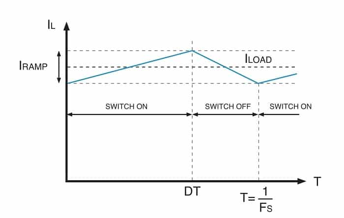

Fig. 2: The ramping waveform of a switching DC/DC converter.
The waveform of the current flowing through the inductor in the case of a buck converter is shown in Fig. 2. It includes an average DC component and an AC component, which is periodically ramping up and down. The DC current equals the DC load current Iload. Under steady-state conditions, the inductor current at the end of the cycle equals that at the start of the cycle.
The controlled switching action results in
Vout = D * Vin (Equation 1)
with D being the duty cycle as D = ton /(ton + toff).
The switching frequency is determined by fsw = 1/(ton + toff), with ton = D/fsw.
Adding up all the voltage drops generated in the circuit during ON time, and assuming that Vsw = 0, this results in
Vin – Vind – Vout= 0 (Equation 2)
If we now substitute Vind = L * di/dt, with di resembling the magnitude of the current ramp Iramp and dt the ON time ton, this will get us to
L * Iramp = (Vin – Vout) * ton (Equation 3)
This has a significant consequence because the right hand side of Equation 3 is constant for a given input-to-output voltage difference, implying the same for the resulting switching frequency and the value of ton. A larger inductance value L equals a smaller ramping current component, while smaller inductance values will lead to a larger current ramp. Driving this to the extreme, if the inductance is chosen to be very small, there may be a current ramp so large that at a low-load current condition, the total current flowing through the inductor could drop to zero for part of the switching period. This condition is called discontinuous mode.
There is another important consideration that must be kept in mind; a smaller inductance, which may be attractive in some applications, leads to a larger inductor ramp current, and this causes a higher ripple to occur on the output voltage. A large Iramp also increases the AC core losses in the inductor. As a general guideline, Iramp should be small compared to the maximum load current; this determines the inductance value L for a given system design.
Now, let’s turn to a key specification in regard to choosing the proper inductance value. It is the maximum peak current through the inductor. In steady state operation, it is
Imax = Iload_max+ Iramp/2 (Equation 4)
Looking at Equation 3, it is apparent that Iramp is independent of Iload. To determine Imax, a more detailed consideration is needed as to how Iramp will vary with different values of Vin after deciding on the values of the inductor L.
Adding up all the voltage drops and with Vd = 0 during OFF time, this results in
Vind – Vout = 0 (Equation 5)
Considering Vind = L * di/dt, with di being the magnitude of the current ramp Irampand dt being the OFF time toff, leads us to
Iramp = Vout * toff/L (Equation 6)
If Vout is constant, Iramp is at a maximum when toff is also at a maximum. This occurs when Vin is at a maximum, and this condition determines Iramp and the maximum peak inductor current (Equation 4).
With the inductance value determined and the maximum current known, this finally leads us to the selection of the appropriate inductor type. Shielded and low-EMI inductors are good choices for densely populated boards, as is the case in new IoT designs. Their advantage is that their magnetic flux is contained within the inductor body, resulting in a lower radiation impact on surrounding PCB traces and components.
As an example, Signal Transformer’s SCRH series of magnetically shielded parts are available with inductance values ranging from 1.0 µH to 180 µH, saturation currents from 0.15 A to 5.0 A, and heights from 1.9 mm to 4 mm. If a larger inductance value is required, the SCxxxxC Series offers values from 10 µH to 1 mH, with saturation currents from 0.045 A to 8 A and heights from 2.92 mm to 7.62 mm. Other series are available for high-current applications as well as unshielded inductors for highest efficiency and robust power handling that include low-profile dimensions.
featured image source: Signal Transformer

