
This article elaborates on properties and selection of capacitors for DC/DC converter applications. The post is based on Würth Elektronik‘s “DC/DC Converter Handbook” that can be ordered from WE website here. Published under permission from Würth Elektronik.
Key Takeaways
- The article discusses the importance of selecting suitable capacitors for DC/DC converters, citing key factors like ripple current and impedance.
- Capacitor ripple current must meet lifetime standards, as defined in datasheets, and influences overall efficiency.
- The paper emphasizes measuring capacitor performance, especially in switched-mode power supplies, to prevent incorrect dimensioning.
- Effective tools like REDEXPERT assist in capacitor selection by considering frequency-dependent behavior and impedance.
- In practice, optimization often requires a balance between capacitor properties and circuit design to meet EMC standards.
The input and output capacitors of switched-mode power supplies are essential components, along with the inductors and the power switches, and should be carefully dimensioned accordingly.
read also: How to Calculate the Output Capacitor for a Switching Power Supply
Almost all the AC current generated by the switching operations in a switched-mode power supply passes through the input/output capacitors. This situation is caused by the impedance conditions in the overall system (power grid – switched-mode power supply – load). On the output side, the load impedance and the impedance of the output capacitor are opposite, whereas on the input side, the power grid impedance (impedance of the voltage source) and the imped
ance of the input capacitor are opposite.
To create standardized test conditions, this power grid impedance is simulated by a power grid simulation in the EMC laboratory. The effective impedance is defined as 100 Ω over a specified frequency range. In contrast, the input capacitor impedance is much lower (typically: < 0.1 Ω). According to the general current divider rule, the simplification applied below implies that the entire AC component is conducted in the low-impedance input capacitor. The corresponding behavior applies to the output capacitor.
This fact gives rise to the two essential but often neglected criteria that apply to capacitor selection in switched-mode power supplies:
- capacitor ripple current: Is the capacitor capable of carrying the AC component throughout its lifetime?
- Impedance: Is the impedance of the capacitor sufficiently low that the voltage ripple resulting from the AC current remains low? On one hand, the voltage ripple can have a negative influence on the circuit function; and on the other, it is indirectly specified by the EMC standards.
Capacitor Ripple Current
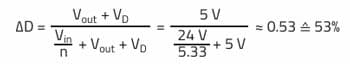
The ripple current permissible for a capacitor’s service life is defined in the datasheet as a function of frequency and temperature. This specification is a result of the capacitor’s maximum permissible internal temperature rise, which leads to aging (capacitance loss, ESR increase). This temperature rise is due to the thermal energy generated by the capacitor’s RMS current IC and the equivalent series resistance (ESR). Often, the negative impact of this heat output on the efficiency of the converter goes unnoticed.
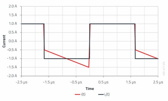
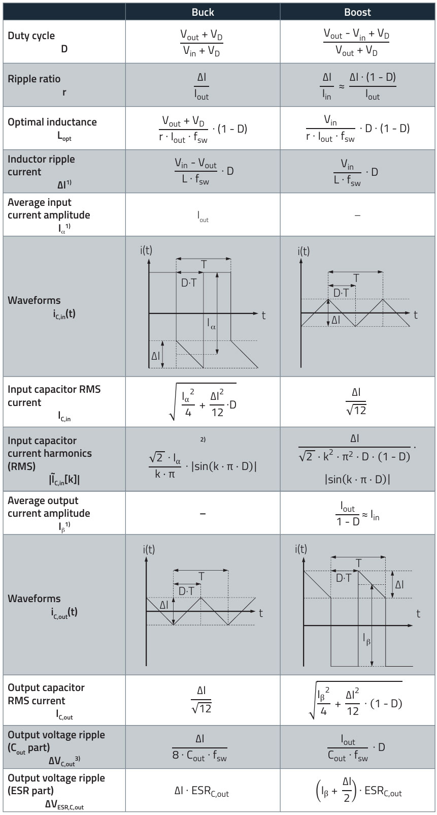
Depending on the switched-mode power supply topology and the position of the capacitor, the time-dependent current curve and thus the rules for calculation the RMS current differ. All currents through the capacitors have in common that in the steady state (periodic process), it is pure alternating current, whereby the current-time areas in the current-time graph above and below the zero-ampere axis are equal in size. It can be quite a challenging task to derive the as sociated time function and to determine the RMS current from it:
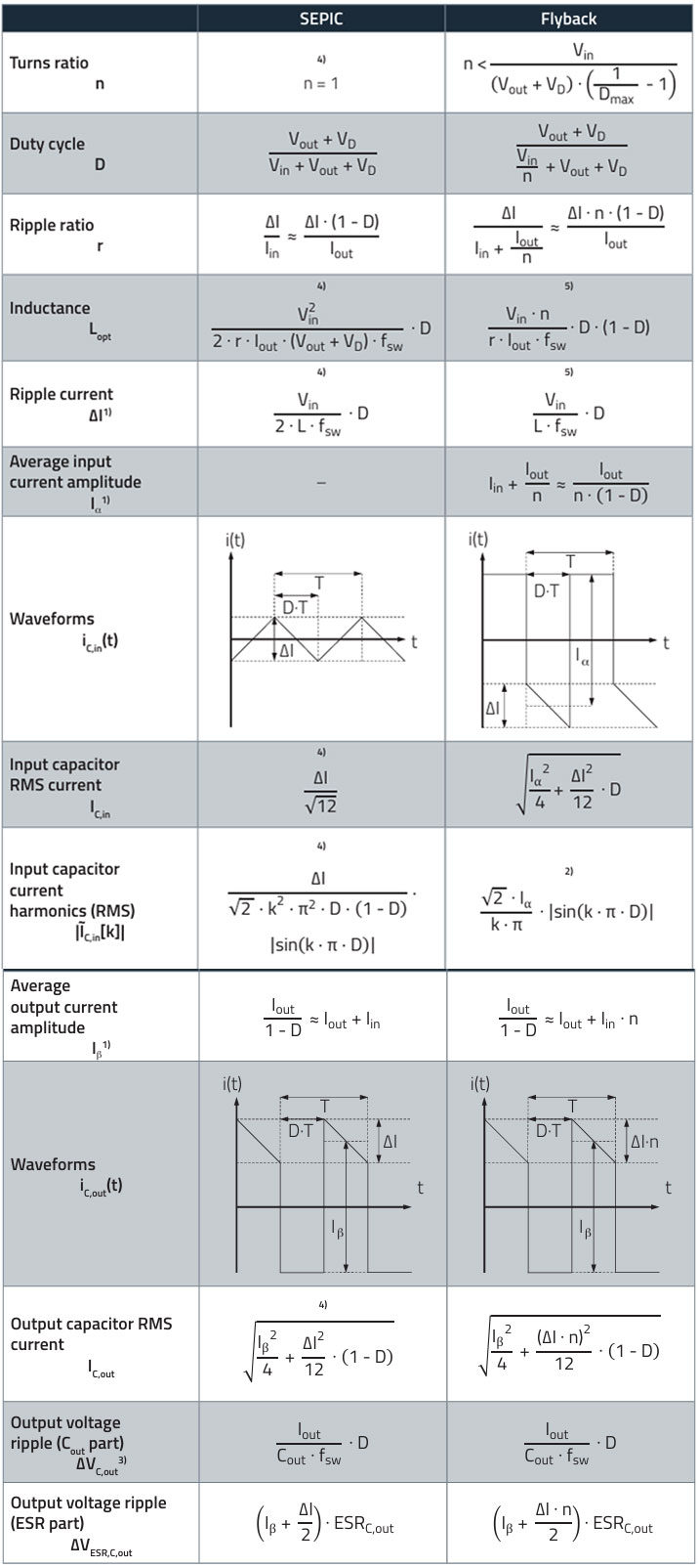
The calculation rules for the typical switched-mode power supply topologies are specified in the power converters basic formulas tables for buck / boost converter Table 1., and SEPIC / flyback converter Table 2. This creates a selection criterion for capacitors to prevent incorrect dimensioning.
The following practical example serves to illustrate that it is worthwhile calculating the capacitor current.
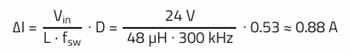
Topology: Flyback converter with synchronous rectifier
- Input voltage: Vin = 24 V
- Output voltage: Vout = 5 V
- Output current: Iout = 5 A
- Switching frequency: fsw ≈ 300 kHz
- Transformer turns ratio: n = 5.33
- Transformer primary inductance: L = 48 µH
This information is sufficient to estimate the RMS currents.
Step 1: Calculation of duty cycle D (see Table 2)
As this is a synchronous flyback converter, the diode forward voltage (VD = 0 V) is omitted in this analysis.
Step 2: Calculation of the ripple current ΔI (see Table 2)
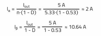
Step 3: Calculation of Iα and Iβ (see Table 2)
Step 4: Calculation of the RMS values ICin and ICout (see Table 2)
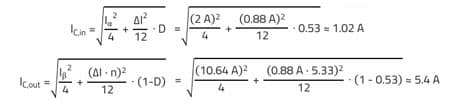
The input capacitor current can be reprinted in this example circuit very conveniently in the frequency range up to 1 MHz with a current transformer (TR2 – WE-CST 749252100) on the oscilloscope. The current transformation ratio of 1:100 and the 100 Ω shunt resistor mean that 1 A is depicted by 1 V on the oscilloscope.
The AC RMS measurement function of the oscilloscope determines an RMS value of 1.13 A for this current curve. The deviation from the theoretical analysis (1.02 A) comes from the actual efficiency of approximately 90%, the tolerance of the components, as well as the measuring method applied with the current transformer.
In practice, it is much more difficult to measure the RMS current. You need a current clamp with high bandwidth (BWcp » fsw), while having the possibility of positioning the current clamp in series with the capacitor.
However, with such a measurement setup you change the impedance conditions and thus the actual measurement variable. This shows all the more that a theoretical analysis is worthwhile.
REDEXPERT effectively assists the developer in selecting capacitors with regard to the ripple current. In the aluminum electrolytic/aluminum polymer capacitor module, the “Specified Max.Iripple” column can be used to limit the selection regarding the ripple current.
Depending on the application, the multiplication factors for frequency (≈ switching frequency) and temperature (≈ ambient temperature) should be included in the consideration.
REDEXPERT Link: we-online.com/HDC_selection_cin
Besides the rated current, restrictions were placed on the selection of the input capacitor in terms of the rated voltage (30 V ≤ VR ≤ 100 V) and assembly type (THT) according to the application. But still more than 100 Würth Elektronik articles fit the bill.
REDEXPERT Link: we-online.com/HDC_selection_cout
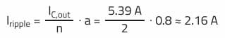
The high RMS current (5.39 A) in the output capacitor indicates that it makes sense to use more than one capacitor. As a 20% capacitance deviation can be assumed in the worst case and an ideal impedance distribution cannot be ensured in the layout, a reduction factor of a = 0.8 should be assumed.
For the ripple current of a capacitor (worst case), the following therefore applies for two output capacitors connected in parallel (n = 2):
Besides the rated current, restrictions were placed on the selection of the capacitors in terms of the rated voltage (5 V ≤ VR ≤ 10 V) and assembly type (SMT).
For the output capacitor, there are still many articles on the shortlist. So, the question arises as to which capacitors are best suited for the application beyond the ripple current consideration.
Capacitor Impedance
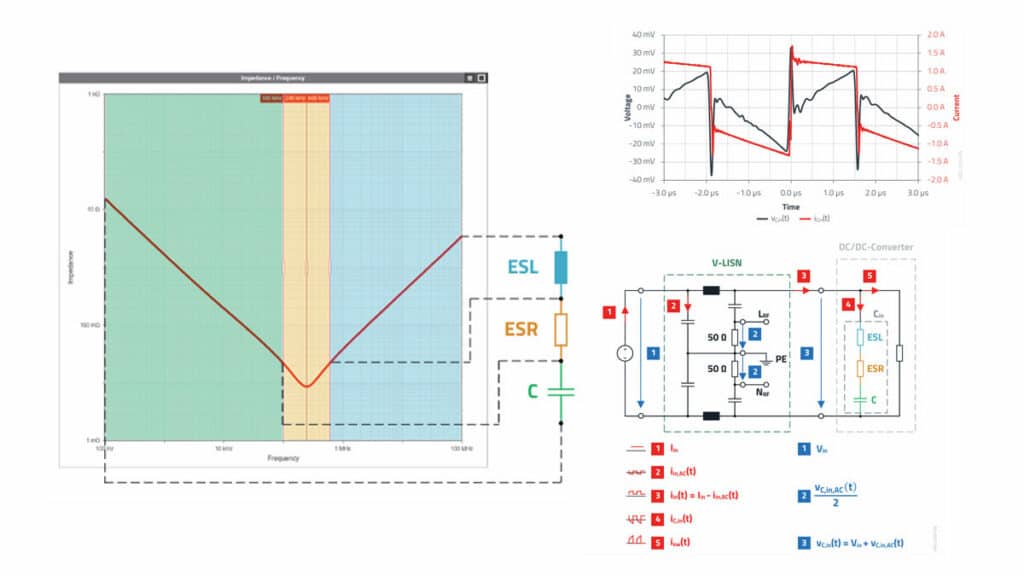
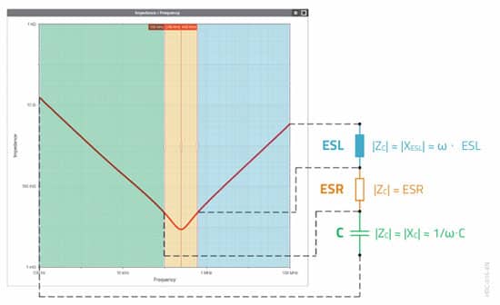
In the case of a capacitor, one automatically thinks of capacitance as the determining component property ( XC = 1 / ωC / VC = Q / C ). This purely capacitive behavior that applies to the ideal capacitor has little to do with reality. In its frequency-dependent behavior, a real capacitor consists of capacitive, resistive, and inductive parts, which can be represented in an equivalent circuit.
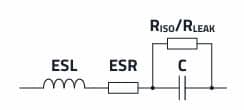
ESL – equivalent series inductance: This combines the inductive parts of the capacitor. These include, among other things, the inductance of the connecting wires and, if applicable, the foil wrap.
ESR – equivalent series resistance: The loss parts are summarized in the ESR. This includes, for example, the ohmic resistance of the connecting wires and the electrode contact. In addition, the ESR characterizes the recharging losses in the dielectric.
RIso / Rleak: The parallel resistor reflects the leakage current in the equivalent circuit and is only of importance in the lower frequency range or with direct current. The low but constant losses from the parallel resistor can be critical for battery-powered applications.
The parallel resistance is neglected in the following analyses.
The following theoretical example is intended to show the potential significance of ESR and ESL on the voltage ripple, shown in the time domain.
Capacitor properties:
ESL = 0.5 nH, ESR = 10 mΩ, C = 100 µF
Converter parameters:
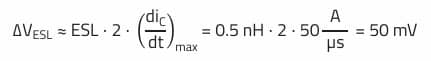
fsw = 300 kHz, D = 0.5 ≙ 50%, ΔI = 1 A, Iα = 2 A, (di/dt)max = 50 A/µs
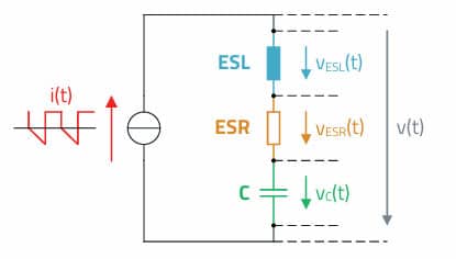
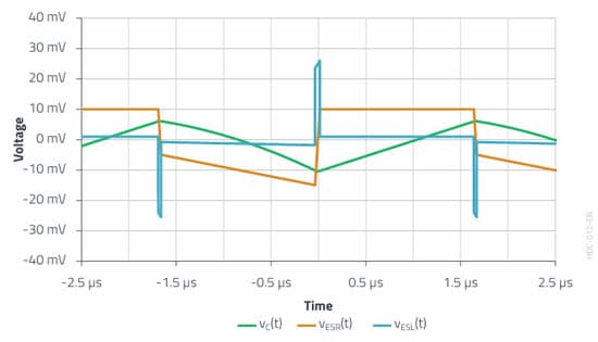
The three figures show how the total voltage waveform v(t) at the capacitor is composed of the individual voltage curves at the equivalent circuit components ESL, ESR and C. Of course in reality, it is not possible to measure the individual voltages from a metrological point of view.
For the voltage at the ESL:
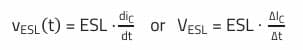
The current (change in magnetic flux) generates an induction voltage at the ESL.
Applied to the current in the example with a slope of 50 A/µs for the rising and the falling edge, this relationship gives rise to a voltage change (peak-to-peak value) of about 50 mV.
For the voltage at the ESR:
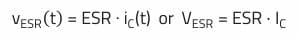
The voltage drop at the ESR is in accordance with Ohm’s law. It therefore maps the current waveform 1:1.

For the voltage at the ideal capacitor:
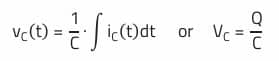
The current-time areas (charge Q = I · t) above and below the zero-amp axis charge and discharge the capacitor. The resulting voltage change depends on the capacitance.
For the current waveform in the example, the voltage change for the charging phase is very easy to determine. Since the voltage change must be the same for the charging and discharging phases, this allows the peak-to-peak value of the voltage waveform to be calculated.
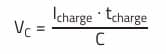
with tcharge= T · (1 – D) and T = 1/fsw
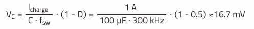
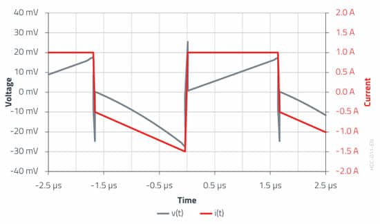
The surprising result is that the voltage drop at the capacitance of 16.7 mV is very low despite the fact that a capacitor with very low ESR and ESL values was assumed.
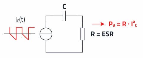
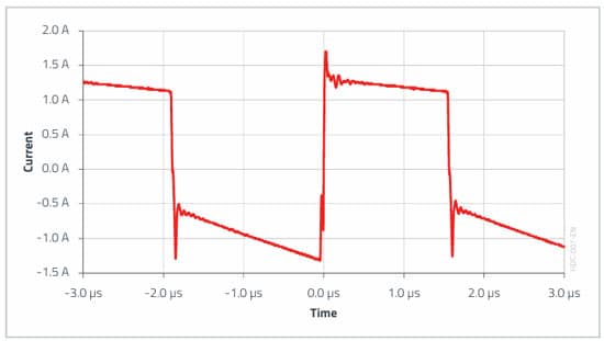
The following waveform of the voltage at the input capacitor vC,in(t) was measured in the example application:
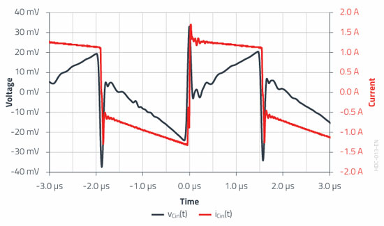
The appearance is in line with the previous considerations. The voltage spikes generated at the ESL during the maximum current change are clearly apparent. This voltage waveform was recorded by the oscilloscope with a bandwidth limit of 3 MHz (10 · fsw). This is necessary because the ESL for the real capacitor is much higher than assumed. Without the bandwidth limitation, it would not be possible to distinguish the ESR and C parts of the ripple voltage due to the dominance of ESL.
But if ESR and ESL are so critical for ripple voltage, why are these values not often specified in the datasheets?
It is not expedient to know the specific equivalent circuit values for a detailed time domain analysis. What the simplified equivalent circuit cannot reproduce is that the equivalent parameters ESR and ESL which themselves are also frequency dependent. For the ESR, this frequency dependence is included in REDEXPERT.
The frequency dependence of ESR is due to the recharging losses in the dielectric, among other things. In practice, the application must be taken into consideration, because a datasheet specification of the ESR, e.g., 120 Hz (or specification of the loss factor DF = tan δ at this frequency) does not say anything in the case of a switched-mode power supply that operates at a switch ing frequency of 300 kHz.
It is much more interesting to know the resulting capacitor impedance for the frequency range evaluated in the EMC laboratory. If the associated frequency-dependent current flow through the capacitor is known, the interference voltage levels can even be approximately evaluated in the EMC lab.
Ohm’s law applies accordingly:
If the interference voltage |V(f)| is to be reduced at a certain frequency, the frequency-dependent impedance (e.g., the impedance of the input capacitor) must be reduced, because the interference current |I(f)| is predefined by the circuit and the output load.
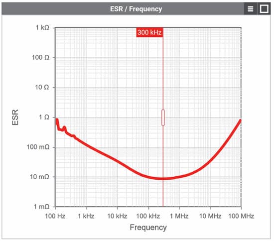
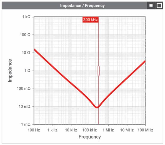
The impedance curve of capacitors required for this purpose and based on measurements is also included in REDEXPERT. The cursor function can be used to precisely determine the impedance at a specific frequency. If the cursor is set to a switching frequency of 300 kHz, an additional column provides the option of sorting the capacitors by the magnitude of impedance at that frequency.
Selection of an optimized capacitor with the help of REDEXPERT:
Step 1:
Use the filter to restrict the rated voltage, ripple current, temperature range, lifetime, and mechanics according to the application.
Step 2:
Place the impedance cursor on the critical frequency (e.g., switching frequency).
Step 3:
Sort the newly created impedance column by size by clicking the column header “Z@300kHz”. The ideal input capacitor (WCAP-PTHT 870135675003) for the application was selected using this method.
Using the impedance curve from REDEXPERT, it is also possible to determine the components for the simplified equivalent circuit. The restriction mentioned above that this model is mainly suitable for frequency-dependent impedance behavior, applies.
For the capacitor impedance according to the simplified equivalent circuit, the following applies:
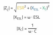
Accordingly, frequency ranges can be assigned to the impedance curve in which the capacitive (falling impedance with rising frequency), the resistive constant impedance over frequency) or the inductive behavior (rising impedance with rising frequency) dominate.
Determining the simplified equivalent circuit parameters using REDEXPERT:
Step 1:
The resonance frequency can be determined using the cursor function. At the resonant frequency, the capacitive (XC) and inductive (XESL) reactive parts cancel each other out. This means that at this frequency, the ESR determines the capacitor impedance.
REDEXPERT Link: we-online.com/hdc_esr
For the article WCAP-PTHT 870135675003 (100 µF/ 35 V polymer capacitor), ESR = 8.7 mΩ is determined at a resonance frequency of fres ≈ 230 kHz:
“Z@230Hz” “8.70 mΩ”
This particularly low ESR value is a distinguishing feature of the Würth Elektronik polymer capacitors.
Step 2:
The ESL can be determined by two methods. If it is important that the equivalent circuit is accurate with regard to the resonant frequency, the ESL should be calculated from the resonant frequency (Method 1). This works well if the resonance is clearly pronounced.
Method 1:
For the resonance frequency the following applies:
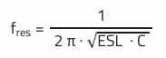
Rearranged for ESL:
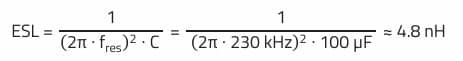
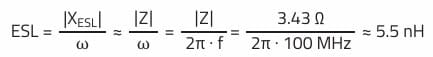
If it is important that the impedance is also correctly depicted for high frequencies in the inductive range, the ESL should be determined with the second method. This method is preferable for electrolytic capacitors with higher ESR, as it is difficult to determine the resonant frequency from the bathtub-shaped curve.
Method 2:
Here the cursor is placed on any frequency in the inductive range up to the end of the measuring range (e.g., 100 MHz).
REDEXPERT Link: we-online.com/hdc_esl
For the article WCAP-PTHT 870135675003 this method gives a value of 3.43 Ω at 100 MHz: “Z@100MHz” “3.43 Ω”.
It is assumed that the impedance in this range is dominated by the inductive reactance, there fore the following applies:
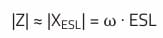
Rearranged for ESL:
Determining Interference current
Up to now, a capacitor optimized for the application was selected and the corresponding impedance curve was modeled and discussed. The frequency-dependent capacitor current is still missing in the calculation of the interference voltage. How can this current be determined?
The periodic capacitor current waveform must be broken down into its frequency components for this purpose. Fourier analysis is the mathematical tool for this.
As the simplified impedance representation does not show the phase relationship, only the RMS spectrum is needed, where the current values are represented as integer multiples (k = harmonic number) of the fundamental (switching frequency).
To keep the mathematical formula manageable, the trapezoidal current waveform i(t) from the previous analysis is approximated as an ideal rectangle waveform i2(t). In other words, a vanishingly small current ripple ΔI and an infinitely steep slope rise are assumed. The following display shows that the error in the lower spectrum is not particularly large. In this example, this particularly applies to the fundamental (switching frequency) and the odd harmonics dominating beyond this.
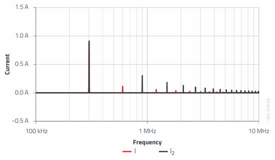
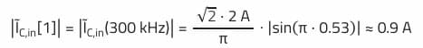
The theoretical example shows that the value of current at the switching frequency (300 kHz) clearly dominates the spectrum with approximately 0.9 A. In relation to the application (flyback converter), the square-wave approximation can be applied to the spectrum of the input capacitor current waveform.
According to Table 2, the following mathematical relationship applies:
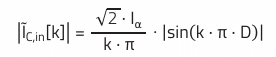
Fundamental k = 1 (switching frequency ≙ 300 kHz):
3rd harmonic k = 3 (≙ 900 kHz):
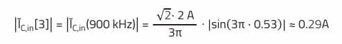
Tip: The calculator must be switched to radian measurement (RAD) for the sine calculation. This procedure can be applied to all other topologies. It is only necessary to select the correct calculation rule for the spectrum according to Table 2.
The following spectrum was obtained using the oscilloscope FFT function from the input capacitor current waveform (see Figure 2.) in the application.
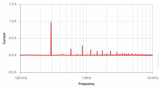
The deviation from the theoretical analysis is explained by the square-wave approximation applied, the neglected efficiency of the converter, and by the signal distortion due to the current transformer.
Nevertheless, the orders of magnitude are correct, especially for the switching frequency (0.98 A compared to 0.9 A) and for the 3rd harmonic (0.28 A compared to 0.29 A). Using the frequency-dependent impedance of the input capacitor from REDEXPERT, the resulting voltage amplitudes can be inferred.
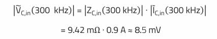
Fundamental k = 1 (switching frequency ≙ 300 kHz):

The deviation from the theoretical analysis is explained by the square-wave approximation applied, the neglected efficiency of the converter, and by the signal distortion due to the current transformer.
Nevertheless, the orders of magnitude are correct, especially for the switching frequency (0.98 A compared to 0.9 A) and for the 3rd harmonic (0.28 A compared to 0.29 A).
Using the frequency-dependent impedance of the input capacitor from REDEXPERT, the result ing voltage amplitudes can be inferred.
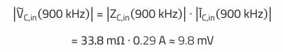
Fundamental k = 1 (switching frequency ≙ 300 kHz):

3rd harmonic k = 3 (≙ 900 kHz):
Can the interference voltage values calculated this way (in dBµV) be equated with the measure ment results of the conducted interference voltage in the EMC lab?
Not quite, because there are several reasons for this.
Reason:
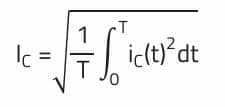
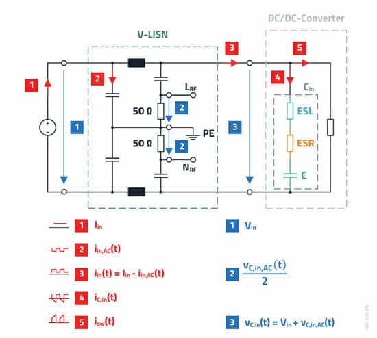
Conducted interference is decoupled from the measuring receiver in the EMC lab with a line impedance stabilization network (LISN). The LISN acts as a low-pass filter for the supply voltage Vin (DC voltage in this case) and as a high-pass filter for the superimposed high-frequency harmonics of the input capacitor voltage vC,in,AC(t).
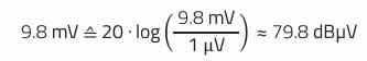
The high-frequency interference vC,in,AC(t) is conducted through capacitors (= DC blocker/AC coupling) to the input of the measuring receiver with an input impedance of 50 Ω or to a 50 Ω terminal resistor. The limits according to CISPR (Comité International Spécial des Perturbations Radioélectriques) 32 (EN 55032) applied in this example require conducted interference to be measured with a V-LISN according to CISPR 16-2-1 (EN 55016-2-1), whereby the LISN is symmetrically structured as shown in Figure 16. and the interference is evaluated separately for L(+) and N(–). The differential-mode interference that occur at the input capacitor is divided by the 1:1 voltage divider (50 Ω : 50 Ω). The amplitude of the voltage at the input capacitor is halved by the V-LISN, which corresponds to subtraction of 6 dB (20·log(0.5) ≈ –6 dB) on the voltage normalized decibel scale.
For the interference voltage |VL,RF| determined in the example application using the LISN, the following applies:
Fundamental k = 1 (switching frequency ≙ 300 kHz):

3rd harmonic k = 3 (≙ 900 kHz):

2nd Reason:
The V-LISN in the EMC lab not only detects differential mode (DM) interference, but also common mode (CM) interference. The common-mode current flows via the reference ground (PE) to the mains terminal where it is divided between channels L and N and is detected as a voltage drop across the 50 Ω measuring receiver impedance. Depending on the frequency and channel dependent phase relationship to each other, the interference amplitudes in the spectrum either add or subtract. This effect is noticeable with equal interference voltage levels (for DM and CM) and in phase with a maximum of +6 dB. Usually, one or the other interference type dominates, which means the addition of interference types in the logarithmic plot goes unnoticed.
If the interference level measured is significantly above the level expected for differential-mode interference and DM filtering (LC filters) does not change this, the dominance of common mode can be assumed.
In the case of non-isolated converters (buck, boost, SEPIC) in the low voltage range, the differential mode conducted interference usually dominates. However, significant common-mode interference can be generated within the application (flyback converter). So, the circuit board for the measurement was configured to minimize the parasitic capacitance from the switching node to the reference ground. The galvanic isolation was also removed for this purpose.
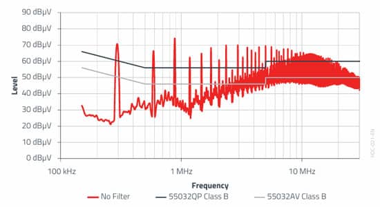
The measured interference levels (Figure 16.) for the switching frequency and for the 3rd harmonic therefore agree very well with the calculation.
3rd Reason
The measuring receiver in the EMC laboratory records the interference spectrum with ‘detectors’. They filter the interference spectrum using a specific method within a defined frequency range (RBW = resolution bandwidth). The limits specified by EN 55032 Class B apply for the frequency range from 150 kHz to 30 MHz, for measurement with a quasi-peak detector (QP) and an average detector (AV) at a RBW of 9 kHz. The RMS spectrum calculated from the Fourier series corresponds to the peak detector (PK) however, for which this standard does not define a limit.
For a periodic signal the following applies:
PK > QP > AV
This means that if the peak values are already below the QP and AV limits, these limits will also be met with the quasi-peak detector or the average detector. For the applications operated with DC voltage it is even clearer. Because with DC voltage there are no “pulse repetitions” below the switching frequency (unlike with a 50/60 Hz AC voltage).
The switching frequency of 300 kHz is far above the RBW of 9 kHz. It is therefore a continuous signal for which:
PK = QP = AV
To summarize: The interference voltage levels calculated at the input of the DC/DC converter should be 4 dB below the AV limit. This analysis includes a 10 dB margin for component toler ances and systematic errors (e.g., due to the rectangular approximation), and 6 dB reduction due to the V-LISN.
The AV limit in this example is 50 dBµV at 300 kHz. The goal should be to achieve a DM interference level of less than 46 dBµV at the switching frequency. The DM interference level at the switching frequency must therefore be reduced from 78.6 dBµV to 46 dBµV, i.e., a further 32.6dB.
Despite careful dimensioning of the input capacitor, it is not possible to achieve a DM interference level below the AV limit value defined by EN 55032 Class B. An additional LC filter (DM filter) is necessary. And with the help of REDEXPERT and manageable math you can come to this conclusion during circuit design, which can prevent an expensive redesign and a second visit to the lab.
Selection of Capacitors for DC/DC Converters: FAQ
Capacitors in DC/DC converters are crucial for filtering, storing energy, and minimizing voltage ripple in both input and output stages. Their performance affects circuit stability and electromagnetic compatibility.
The essential factors include ripple current rating, impedance at working frequency, equivalent series resistance (ESR), equivalent series inductance (ESL), and lifetime under operational temperature and frequency conditions.
Ripple current rating defines the capacitor’s ability to handle alternating current (AC) without excessive heat generation or premature aging. Insufficient rating can result in reduced efficiency and early device failure.
ow ESR is desired to minimize power losses and heating, while low ESL is important to limit inductive voltage spikes, especially at high frequencies. Both parameters are frequency-dependent and impact ripple and interference.
Using capacitors in parallel shares ripple current load and reduces total impedance, improving voltage stability and lifespan of each capacitor.
Oscilloscope and frequency analysis (FFT) measure ripple current and impedance in laboratory setups, but theoretical calculations using datasheet values are reliable for initial design.
Yes, standards like EN 55032 and usage of Line Impedance Stabilization Network (LISN) are important for conducted EMI measurements and compliance.
Online simulation tools by leading manufacturers provide filters and calculation options for ripple current, impedance, voltage, and temperature, helping designers choose optimal capacitors for their application.
How to Select Capacitors for DC/DC Converters
- Define Circuit Requirements
List input/output voltage, current, switching frequency, and desired voltage ripple.
- Calculate Ripple Current
Use converter topology formulas (Buck, Boost, SEPIC, Flyback) to estimate RMS ripple current for input and output capacitors.
- Estimate Required Capacitance
Determine capacitance values based on voltage ripple and circuit stability needs.
- Specify ESR and ESL Limits
Set maximum ESR and ESL values considering converter frequency to minimize losses and high-frequency noise.
- Select Capacitor Types
Choose suitable technologies (ceramic, polymer, electrolytic) matching lifetime, voltage rating, mounting type (SMT/THT), and cost constraints.
- Check Datasheet Ratings
Verify maximum ripple current, ESR at operating frequency, and lifetime specification in the datasheet for each candidate capacitor.
- Utilize Design Tools
Apply available simulation tools or Spice components real PN libraries to filter and sort capacitors by impedance, rated current, voltage, and frequency suitability
- Test and Validate Performance
Conduct lab measurements using oscilloscopes and LISN setups for actual impedance and ripple current verification; compare with theory.
- Optimize with Multiple Capacitors
If ripple current or voltage ripple exceeds limits, consider parallel capacitor arrangements to share current load and further reduce impedance.
- Ensure Compliance with EMC Standards
Confirm selected capacitors help meet EN 55032 (CISPR 32) EMI limits and comply with required testing using LISN and appropriate laboratory procedures.
Read also the related articles in this series:
- Selection of Storage Inductors for DC/DC Converters
- Input filters for DC/DC converters
- Switching vs Linear Power Converters Compared
- Buck Converter Design and Calculation
- SEPIC Converter Design and Calculation
- Boost Converter Design and Calculation
- Flyback Converter Design and Calculation
- Fly-Buck Converter Explained and Comparison to Flyback
- LLC Resonant Converter Design and Calculation
- How to Calculate the Output Capacitor for a Switching Power Supply

