source: elektronikNet.de article
Prof. Dr. Leo Lorenz, Chairman of the Advisory Board of PCIM Europe, talking to DESIGN&ELEKTRONIK power expert Ralf Higgelke about assembly and interconnection future and which issues will dominate the power electronics in the coming years as the main PCIM conference topic.
Assembly and Interconnection will be the Issue of the Future
DESIGN&ELEKTRONIK: If you take a look at the conference schedule of PCIM Europe 2019, what do you think are the main topics this year?
Professor Leo Lorenz: At the conference, we will illustrate exactly in which direction power electronics will evolve in the next several years. For me, therefore, the focus lies on three fundamental subjects: firstly, wide band gap technologies, and secondly, highly reliable embedded power integration. Ultimately, the latter topic encompasses the design of power modules for extremely fast switches, new materials for good insulation with excellent heat dissipation, and assembly and interconnection techniques. From my point of view, this will dominate the discussion over the next maybe ten years. Thirdly, one main focus is »High-Tech China«.
Let’s take a more in-depth look into these three topics. What do you think is new regarding wide bandgap technologies?
At device level, gallium nitride on gallium nitride is an interesting subject. All solutions currently available on the market use a standard silicon wafer as carrier to deposit gallium nitride on it and create the transistor. However, due to the different coefficients of thermal expansion and the different crystal structures of silicon and gallium nitride, the interface between these two materials is the weak spot. In order to overcome this, stress or buffer layers are built in as intermediate layers.
At PCIM Europe, Panasonic will show that GaN on GaN (right) is economically viable even on 150 millimeter wafers. This offers compared with the traditional GaN-on-Si approach (left) new degrees of freedom with even lower switching losses and a stable, low switch-on resistance.
Gallium nitride on gallium nitride has not been taken seriously. Until now, this approach has been considered to be far too expensive, and the wafer diameter was limited. But Panasonic is going to show us, that GaN on GaN is economically feasible even on 150 millimeter wafers. This offers new degrees of freedom with even lower switching losses and a stable low switch-on resistance. This might, for example, reduce the output capacitance significantly, as the thickness of the material can be varied more easily. By lowering the output capacity, the dynamic losses are also reduced as well. Additionally, the turn-on resistance would be more stable, because the number of electron traps in the bulk of the semiconductor material would decrease significantly. This in turn would reduce conduction losses.
What about integration with gallium nitride?
This is also becoming increasingly important. We have a couple of papers, in which the entire control circuit, besides the power stage, was realized in GaN. Although this idea is not fundamentally novel, due to the fast switching of these transistors this topic is becoming much more relevant with respect to silicon. A completely new approach has been developed by the University of Stuttgart and the Fraunhofer Institute IAF in Freiburg. They are working on integrating the entire closed loop control system into gallium nitride. Nowadays, the power and control elements are separated on two individual chips in one package, but in future this will certainly be integrated monolithically onto one single chip.
Is there anything new to report about silicon carbide?
In this respect, I see a continuous but nevertheless substantial progress, but no dramatic leaps. Now the second generation of components is emerging.
On the one hand, we have the devices with a blocking voltage of up to 1200 volts. There the on-resistance is split into two more or less equal parts: the drift and the channel resistance. Currently, the focus lies on reducing the channel resistance. There are several interesting approaches to the so-called »channel engineering«: It involves the passivation, the thickness of the oxide layers and the trench-gate structures, while considering the control of the electric field strength in the cell and edge structures.
On the other hand, one trend in silicon carbide leads to higher blocking voltages. We will see some new approaches at the conference. A SiC device for 3.3 kilovolts and 1000 amps with a sintered copper chip surface for excellent short-term overload behavior and many load cycles will be presented. Taking the example of a SiC switch for ten kilovolts, the challenges of the necessary insulation techniques combined with good heat dissipation will be demonstrated. And for medium-voltage applications, a SiC switch in a cascaded topology and its dynamic behavior will be presented in detail.
However, it is important to note, that, in addition to the wide bandgap technologies, there are a number of important advancements with silicon devices. At PCIM, for example, new approaches will be shown for reverse-conducting IGBTs and specifically optimized IGBTs for e-mobility or multi-level topologies for renewable energies; their electrical and thermal behavior will also be discussed.
Novel Power Module Design
You said that assembly and interconnection technology would be the dominating topic of the next decade. Tell us more about it.
Prof. Leo Lorenz: With these very small and at the same time very fast switching chips, the first major challenge is to deal with this high power density in the chip package. The second challenge is to handle the extremely fast voltage and current transients, both in the module as well as in the end system.
Let’s consider the high power density in the package first. It is primarily a matter of effectively dissipating the thermal losses. In addition to the materials already known, silicon nitride, a ceramic material, is becoming more and more popular as a circuit substrate. A further aspect in the area of packaging is contacting the chip with the substrate of the module. The objective is to increase the lifetime, especially when the application has to handle many load cycles. Therefore, at the conference we will discuss various techniques such as silver sintering as well as other novel soldering techniques.
A weak spot in assembly and interconnection techniques is always the thermal junction of the heat sink to the base plate of a module. Do you see any progress there?
Yes indeed. Until now, thermally conductive pastes or foils have been used there. Over time, however, these pastes are squeezed out and leave voids, or air penetrates between the film and the heat sink or base plate. These air voids significantly increase the thermal resistance and thus limit the lifetime of the module.
In cooperation with Fraunhofer researchers, Rogers will present an outstanding new module design with a low-inductive multilayer ceramic substrate with integrated active cooling. The switches are mounted on an insulating ceramic substrate as usual to dissipate the heat. However, a thick copper plate is placed directly underneath in order to absorb the heat and to spread it. This plate is followed by another ceramic layer for insulation. Next comes the newly designed heat sink with integrated liquid cooling, which is attached by hard-brazing. Finally the whole module is molded.
The heat sink is now part of the module housing. This eliminates the interface between the base plate and the heat sink, which is critical for heat dissipation in conventional modules. Depending on the system developer’s expertise, the thermal resistance of this interface accounts for up to 70 percent of the total thermal resistance from the chip to the heat sink, making it the most critical part of the entire system.
What about the other challenge, the fast transients in current and voltage?
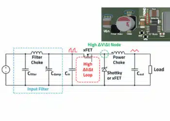
There the way is to minimize the area of all the loops, in which the current commutates – mainly the so-called »hot« loop with the DC-link capacitor and the power transistors. Even here, the Rogers and Fraunhofer solution just mentioned offers a new solution. The central copper layer shown in the picture has the task to spread the heat, but at the same time to carry the current to the DC-link capacitor. The transistors are connected directly to the surface of the module. Thus not only the area of this hot loop becomes very small, but also an additional RF capacitor with a resistor can be placed close to the switches. Thereby the RF energy generated by the fast switching of the switching cell is »extinguished« locally at the same place. The large DC-link capacitor is then responsible for the real energy storage, but it is no longer stressed by the fast switching transitions.
And this approach also addresses a third issue: Due to the fast switching, the control must also be connected as short as possible to the switching cell. This new encapsulated module is connected to the top through vias, so that the control and protective circuitry can be placed close to the switches. Thus it is possible to control the switching process oscillation-free and to detect and switch off a short circuit within the shortest possible time.
In a very interesting paper, researchers from the University of Bayreuth discuss a new concept of detecting and switching off a short circuit. Until now, the detection methods were dimensioned in such a way, that the short circuit was detected not before two to three microseconds, and switched off after about four to ten microseconds – depending on the switch technology and performance level. This is adequate for silicon transistors in conventional designs and chip sizes, but far too slow for wide bandgap switches and new fast-switching silicon transistors. As soon as the transistor is switched on – the current is still rising – it is possible to detect, whether the system is operating as normal or whether a fault is to be expected – for example, a short circuit – and the control circuit must therefore react accordingly. However, it must also be ensured, that the short circuit detection does not respond to any oscillation during the switching process. An appropriate electronic filter as to suppress all these oscillations without disabling the protection features. After all, a short circuit has to be detected reliably at all times.
In summary, we have fifty papers solely dealing with future module technologies, new materials for excellent heat dissipation with simultaneously good insulation as well as assembly and chip bonding techniques. This is the biggest single topic this year. And I am absolutely sure that this will continue for the next ten years.
The third area you mentioned is »High-Tech China«. You have lived and taught in China for many years. Recently you observed something. Tell us more about it.
The Chinese company CRRC has transferred the IGBT technology of Dynex Semiconductor [acquisition in 2008; editor’s note] to China. In the beginning this was a bit bumpy, but today CRRC has a state-of-the-art wafer fab and an excellent research institute, including a lab for power semiconductor devices. In that laboratory, a new generation of IGBTs has been developed which comes very close to what the market leaders have today.
This refers on the one hand to the high cell density in trench gate technology. In modern IGBTs, not all gates are electrically connected. Among other things, these passive gates serve to adjust the electron-hole plasma in the bulk of the silicon correctly and to manage the controllability of the transistor. The market leaders have been doing this for quite some time, but CRRC has now also implemented this in an excellent way in their lab.
On the other hand this refers to the surface metallization with thick copper layers, a step which has taken CRRC now, too. These copper layers are used as heat buffers for short overload conditions, and due to the copper wire bonding the IGBTs are able to withstand many more load cycles. This increases their lifetime up to five to ten times.
China is on the right track. I therefore still believe that we have to keep on working hard to stay ahead or at least be able to keep up. There is one thing we should not forget: If something has been proven as feasible in the laboratory in China, then the time to market for the first products based on it is usually much shorter than with us. Six or seven years ago I had already stated – and I have to repeat myself –, that Made in China 2025 has already outperformed us in specific areas of power electronics.
This is also reflected in the number of papers we received from China. At PCIM Europe there will be ten presentations from Chinese universities, research institutes and companies this year. This number has increased dramatically. At other conferences, up to 50 percent of all abstracts today originate from »Greater China«.
Processing on 300-mm Wafers and Special Sessions at PCIM
China is the most important single market for Infineon. Nevertheless, in spring 2018 the company decided to build a brand new 300-millimeter fab in Villach, Austria. This is an important sign for Europe, isn’t it?
Prof. Leo Lorenz: Absolutely! And I am very pleased, that high-tech like this will help to strengthen Europe as competitive location. To operate such a wafer fab entails a very high level of expertise in the manufacturing processes, the equipment, the test procedures and eventually also in the education at the universities.
It is also an important message to power semiconductors in general. Processing 300 millimeter wafers is completely different from processing smaller diameters. It’s no longer possible to grow the crystal in the usual way, and other processes to manufacture such wafers are needed. Defect densities, doping profiles and so on play an important role. Many things are different.
Initially, no one had taken Infineon for serious. However, the Dresden plant has been manufacturing large quantities of these large diameter wafers for quite some time now. And now other manufacturers are also following suit. STMicroelectronics has announced to manufacture on twelve inches. There was a meeting on this subject in Japan. And the Chinese also want to jump on that bandwagon.
It’s incredibly difficult to handle and process such large thinned wafers, isn’t it?
Correct. The transfer of the wafer diameter from 150 to 200 millimeters was relatively simple, because the process technology remained the same. But the leap from 200 millimeters to 300 millimeters – that’s a completely different world.
Imagine a pizza that is 100 micrometers thick. This is like aluminum foil, which has to be processed precisely in fractions of a micrometer! Infineon really did a pioneering job in this area, doing the preliminary work and developing the entire manufacturing and handling technology together with the equipment manufacturers (see [2]; editor’s note).
The fact that the competitors also now want to produce on 300 millimeters is, of course, very pleasing to Infineon. It is much more difficult to convince wafer suppliers to produce wafers in such large diameters, if there is only one customer.
Which special sessions are scheduled at PCIM 2019?
In the advisory board we agreed on four special sessions, all very important future topics: DC networks, solid-state transformers, smart power electronics and functional safety in drive technology.
There is already an important application for DC power grids today: server farms. These are lower voltages – currently 24 volts, but tomorrow 48 and 380 volts. However, the development will not stop there; we are also discussing medium voltages up to maybe six kilovolts. There are already several pilot projects.
Despite all their advantages, such DC grids pose their own challenges, which are still largely unsolved; these include disconnection in the event of a fault and other safety-related issues. With alternating current, this is much easier, because the spark is automatically extinguished, when the current crosses zero. By its nature, this is not the case with direct current. Therefore, hybrid approaches are discussed, combining a mechanical switch with a semiconductor switch – the semiconductor for the dynamic phase, the mechanical switch for the steady state.
Wasn’t there also a special session on solid-state transformers last year, too?
Prof. Leo Lorenz: You are right, but up to now this topic has been perceived too negative, especially by the utilities, which are very conservative. Of course they are afraid of blackouts, and a 50 Hertz transformer is unrivalled cheap and robust – even a lightning strike is usually no problem. There is now a pilot project in Scotland, where a »smart« grid is to be set up parallel to the existing power grid. The 7,800 solid-state transformers to be installed by 2030 are estimated to save 62 million Pounds Sterling [approx. 71 million Euros, editor’s note] and 523 kilotons of carbon dioxide. By 2050 the figures are projected to be 528 million pounds and 2032 kilotons of carbon dioxide, when 36,270 solid-state transformers are to be connected to the grid.
Another very good application for such smart transformers are trains. There – depending on the individual country – the mains frequency is only 162/3 Hertz. So the transformer fills almost the whole locomotive. A corresponding solid-state transformer is only one tenth as big. This would allow the drive and the power electronics to be distributed in the train, and the locomotive is gone. But also there the life cycles are very long. So it will take some time, until smart transformers are actually used in trains.
Generally speaking, one could say, that in today’s AC grids, solid-state transformers have little prospects because of the missing proof of robustness and their costs. In DC grids however, they are already required today. One example is data centers for banking or other enterprises. Most of these are powered directly from the medium-voltage grid, and solid-state transformers offer significant advantages there. Additionally, I can imagine a very large number of applications in the factories of the future, shopping centers and the entire charging infrastructure for e-mobility.
One special session is named smart power electronics. What do you mean by that?
Let’s take a standard inverter as an example. The actual power electronics, in other words the transistors and the topology, remain almost the same, as does the control and drive circuitry. What is new is communication – both to the inside as well as to the outside.
Regarding communication to the inside, for example, the focus is on protecting the inverter, optimization and diagnostics. Communication to the outside world is about maintenance, process optimization and lifetime prediction. Especially when predicting the lifetime, it is necessary to record and process ageing relevant parameters and make them available to the operator.
Limited Availability of SiC Raw Wafers and Gallium Oxide
Let’s turn to another hot topic: the limited availability of SiC raw wafers. This could inhibit the proliferation of this technology. Do you agree? What can be done about it?
This is a big issue indeed. Basically, we are dealing here with a chicken-and-egg problem: The manufacturers of raw wafers would have to invest massively in expanding their manufacturing capacity today, without having the corresponding sales volumes. It’s also about wafer diameters. Currently, most of these have a diameter of 150 millimeters, but it’s necessary to switch to 200 millimeter wafers. This is a time-consuming process with silicon carbide – not only in order to reduce the defect densities, so that the chip yield is commercially justified. Silicon carbide is slowly grown from the vapor phase in an energy- and thus cost-intensive process. Silicon, on the other hand, is grown relatively quickly from a melt. This means that the wafer price for silicon carbide will never be the same as for silicon. So who is making the first step?
This is why semiconductor companies like Infineon and STMicroelectronics have signed long-term supply agreements with Cree or acquired SiC raw wafer manufacturers such as Rohm with SiCrystal or STMicroelectronics with Norstel.
This is a good way – the only one, that’s making sense to me. You have to send out a strong signal to the manufacturers of raw wafers about the sales volumes they can expect, so that they can ramp up their manufacturing capacities accordingly.
But there are so many issues still left unsolved with silicon carbide. No one dares to take the full risk of investing on a large scale. Currently, the market is still very small. In addition, we still have not enough basic data on lifetime reliability. We need completely novel assembly and interconnection technologies compared to what we currently use for silicon. So there are still many issues to be addressed in order to exploit the full potential of silicon carbide devices. In this context we should not forget that we have to understand and be able to control these small, extremely fast switching chips both in their package and in the system. This affects thermal management, chip contacting techniques to increase load cycle resistance, fast transitions in current and voltage in the switching cell, as well as extremely high switching frequencies at the consumer, especially when inductive loads or filters are involved.
Another wide bandgap material is currently causing excitement: At the end of 2018, Japanese researchers presented a complete ion implantation process for gallium oxide (Ga2O3). What is your assessment of the future prospects of this semiconductor material?
Obviously, this is an interesting approach. And the Japanese are working hard on this technology. But you have to keep in mind that the band gap at gallium oxide is 4.8 electron volts and the breakdown field strength is eight megavolts! For comparison: with silicon carbide, it is »only« 3.3 electron volts and 3 megavolts per centimeter, respectively. This means that it would be possible to build an 800-volt device in gallium oxide, whose drain and source terminals are just one micrometer apart. But this is an utopian idea, because the semiconductor has a passivation applied to it – and that passivation as well must be able to withstand these extremely high field strengths. How do I get the field plates over it? How can I control the electric field? These questions are still totally unanswered.
This means, even though it may soon be possible to manufacture such devices, the enormous potential of the material cannot be exploited at all. Even field strengths of 3.5 megavolts per centimeter cannot be absorbed by passivation today. For safety reasons, the structure sizes of GaN devices are currently some ten micrometers and larger.
But this is definitely an interesting way to go. I don’t want to belittle that. I was in Kyoto back in January and took a look at it. But there is still a long way to go before the enormous potential of this material can be fully exploited.
Professor Lorenz, thank you very much for taking the time.
The interview was conducted by Ralf Higgelke.


