


source: Microwaves&RF article
May 19, 2016 Paul Davidsson, Microwave Distributors Company | Microwaves and RF
Understanding the impact of selecting different materials and manufacturing processes can separate standard high-power resistive components from those designed and tested for true high-reliability applications.High reliability and long lifetimes, two product attributes that tend to go together, both can be enhanced through the thoughtful selection of materials for the design and fabrication of a high-frequency component. A 250-W termination will serve as an example to demonstrate how following proper design guidelines and how standardization of high-power testing methods aid in material selection for reliable, long-lasting high-power components.
Accelerated life testing, where a component is subjected to various operating conditions that may inevitably cause it to fail, can provide insight into how to make its next design iteration more robust and reliable. To better understand design and process issues that may ultimately limit product reliability, particularly for high-power, flange-mounted attenuators, resistors, and terminations, a 1000-h cyclic burn-in methodology was developed to address catastrophic failures.
Accelerated Life Test Specifics
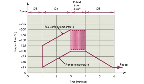
The test procedure was developed to evaluate components for high-reliability (hi-rel) applications, but has merit when applied to new and existing component designs for both commercial and military use. The lifespan of these components depends solely on the end use of the product; e.g., it is known that steady-state operation will ultimately yield the highest reliability when a component is operated according to recommended limits (Fig. 1). In contrast, reliability will be compromised when components are subjected to operation that involves on/off power conditions and temperature cycling (Fig. 2).


The testing resulted in two catastrophic failures, which were identified as fractured beryllium-oxide (BeO) ceramic chips. Such failures can then be correlated to a “root cause” analysis and included in a report that summarizes the cause of the failures. This study helps address materials and processes that could have an impact on failures occurring with present and future component designs. The results have also identified the need for possible design modifications to increase reliability and lifespan.
Digging into Design
During the design phase, the following recommendations apply to high-power resistive devices: reviewing and understanding a customer’s specifications; knowing the maximum operating frequency, the maximum VSWR, and the minimum and maximum operating temperatures at full rated power; knowing pulsed-signal requirements, including pulse width and duty cycle; knowing the power derating specifications; and knowing the power and temperature-cycling requirements.
Selection of materials is critical when designing and developing a high-power resistive component for specific customer requirements. One starting point is deciding which ceramic material can serve as the building-block material to meet a customer’s electrical and thermal design requirements, and whether the design should be fabricated as a thick- or thin-film device. If thin film, should it be based on tantalum-nitrate (TaN) or nickel-chromium (NiCr) films, typically deposited on an alumina, aluminum-nitride, or beryllium-oxide substrate? In addition, if NiCr material is chosen, does the application (such as a high-power pulsed circuit) require any sort of metal reinforcement, such as nickel?
Materials selection also extends to the device flange—it should meet various thermal requirements, such as a coefficient of thermal expansion (CTE) that is well matched to the other materials selected for a hi-rel component. In addition, decisions must be made on the flange plating material, such as inter-metallic materials, and solder or brazing material used to attach a chip component to a flange-mount package. Other materials selection requirements involve whether chip plating will be needed (depending on the solder or brazing requirements) to meet the requirements of a particular application.
Developing a high-power passive component will involve the calculation of an optimum film topology for handling the required power levels while still meeting the RF/microwave performance specifications. It will also necessitate thermal analysis and simulation of the material stack-up per customer requirements using modern computer-aided-engineering (CAE) software simulation tools, as well as simulation of the electrical performance, such as insertion loss, return, loss, and VSWR.
Along with proper materials selection, the choice of manufacturing process should be based on meeting the design goals and customer requirements for a particular component. In addition, test procedures should be formulated in support of characterizing a component for the performance goals set during the design and materials selection stages of a product’s development. It’s crucial that test fixtures be designed for accurate testing of the manufactured component. Also, the fixtures should be able to deliver accurate data consistently throughout the validation process, since this data will determine the success or failure of achieving the design goals. All test data should be recorded, compiled, and incorporated in a validation report that is available for future use.
Validating a Design
For a high-power resistor or termination, two main design considerations can impact the hoped-for long-term reliability of the component: the component being subjected to high temperatures that exceed the limits of the component’s materials, causing reliability issues; and excessively high temperatures being sustained for a long-enough duration that results in damage to the component, or complete failure.
For such a passive component, when power is dissipated, the temperature gradient through the ceramic, solder, flange, and thermal compounds used to construct the component, along with the CTE mismatches among these materials, creates mechanical stresses whenever CTEs are significantly different. The solder attachment of the chip to the flange is subject to fatigue cracking with repeated exposure to stress. A robust design can withstand any fatigue caused by cycling on and off and will not degrade and fail over time.
Material selection is critical for hi-rel components so as to avoid thermally induced stresses that can cause failures. For steady-state operation, a standard material stack-up is normally sufficient. However, when a component must handle power and temperature cycling, solder and flange material selection is critical for high reliability (Fig. 2).
Two cases were used to explore the effects of material selection. In the first case, the material stack-up thermal resistance is 0.1580°C/W with a Δt gradient of +39.5°C at 250 W, resulting in an approximate film temperature of +139°C. This is well below the industry-standard limit of +150° to +180°C. Although the junction temperature (θjc) is very good, the CTEs of the materials differ significantly, resulting in mechanical stresses that will eventually lead to component failures. In the second case, the thermal resistance is 0.2036°C/W, which is higher than the first case, with an approximate film temperature of +150.9°C. This is still within the preferred limit, but the CTE of the material stack-up is almost identical to the first case. Nonetheless, the second case’s material stack-up has the advantage of sustaining higher reliability and a longer life span.


 and understanding differences in thermal flow (b) through different materials in the component.")


Power testing involves two phases. The first phase is intended to verify the film topology of the termination and its power-handling capability for the intended maximum power levels of 250 W. During this test, a component is subjected to full (dc) input power while maintaining a flange temperature at +100°C (Table 1, again). The test runs for 30 min. The temperature of the resistive film is monitored (Fig. 6) to verify that the maximum operating-temperature boundary limits are not exceeded. If the resistive film stays within the boundary range, and no damage is evident to the film, power testing can proceed to the second phase.

Power-test cycling begins with a device under test (DUT) at room temperature (+25°C). Full input power is then applied to the DUT and the flange temperature is raised to +100°C and maintained at that temperature. Once the flange temperature stabilizes at +100°C, the DUT is pulsed with 10 cycles of power-on, power-off operation. This pulsing consists of full power on for 3 s and then zero power for 3 s. After 10 cycles of pulsing, the power to the DUT is turned off and the DUT is cooled down to +25°C. This process is repeated 300 times (Fig. 7, again).

In most cases, standard materials and manufacturing processes are suitable for producing standard high-power passive components. When higher-reliability performance is required, materials and manufacturing processes should be selected with the properties that can provide the target reliability for a given set of operating conditions. Cost of manufacturing the component should also be a design consideration. For high-power components that will have power and temperature cycling as part of the operating conditions, the use of closely matched CTE materials is paramount for long-term reliability, especially in high-power, hi-rel applications like military radar and communications systems.
Editor’s Note: The author has been involved in the development of new product lines of attenuators, resistors, and terminations based on the design methodologies presented above, with enhanced reliability for all commercial and hi-rel applications. The new product lines will be available in the June 2016 timeframe.
Paul Davidsson is President of Microwave Distributors Company, 9020 Kimberly Blvd., Boca Raton, FL 33434; (561) 948-2164, (800) MD-SHELF (800-637-4353).
Bibliography:
Paul Davidsson, Application Note C-36, RF Power Components, 1996.
Anaren Microwave, Application Note ANN-8801, Rev. A, “Thermal Power Testing methodology for Chip, Flange, and PCB-Mounted Resistors.”
Barry Industries, “Finite Element Analysis of a High Power Resistor,” April 1996.
Barry Industries, “Pulsed Power Application Note.”
Tong Hsing Electronic Industries Ltd., “Key Process for Power Chip Attachment,” May 11, 2009.
Mini-Systems Inc., Thick-Film Div., “Anatomy of a High Reliability Chip Resistor.”
American Technical Ceramics, “Engineering Guidelines: Design, Test, and Measurement,” 2004.