


Source: Sensors mag article
Integrated passives are nothing new as they’re long established and well understood. When standalone discrete passives or even integrated passive networks are included as part of a chipset, then routing parasitics, device compatibility, and board assembly considerations will require careful design management. While integrated passives continue to have a strong presence in the industry, their most significant value begins to be realized only when they are included in system in package applications.
by Mark Murphy, product marketing engineer with Analog Devices’ Precision Converter Group in Limerick, Ireland and Pat McGuinness, product engineer at Analog Devices
A new integrated passives technology initiative (iPassives) began at Analog Devices several years ago. Its aim was to deliver passive components, diodes, resistors, inductors, and capacitors that could enable ADI to encompass more of the signal chain while overcoming prior limitations and complexities of the existing approaches of adopting passive components.
From the designer’s perspective, iPassives is a flexible design tool that enables the design of system solutions with best-in-class performance and robustness in exceptionally short development cycle times. ADI has many signal conditioning ICs whose performance is enabled by the unique silicon fabrication processes it has at its disposal. Without the complexity of having to develop highly complex integrated processes, ADI can leverage the diversity of its existing offering to produce plug and play systems that have exceptional performance characteristics.
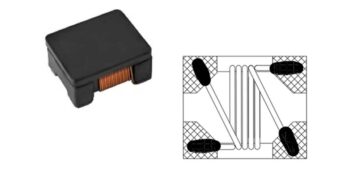
Integrated passives technology is being used to tie this all together in highly customizable networks and packaged up via system in package technology to create μModule devices that are fully qualified, tested, and characterized. Systems that were previously board-level solutions can now be reduced to what appears as a single device. Customers can now get complete solutions with excellent out of the box performance, short development cycles, and cost savings— all in very compact packages.
Passives Technology
Passive components are unpowered devices that give a relatively simple relationship between current and voltage. These components are resistors, capacitors, inductors, transformers (which are effectively coupled inductors), and diodes. Sometimes the current-voltage relationship is very simple, like in a resistor where the current is linearly dependent on voltage. For a diode, there is a direct relationship between current and voltage, but the relationship is exponential. In inductors and capacitors, the relationship has a current and voltage transient dependency. Table1 shows the formulae that define these relationships for four of the basic passive components:
 Table 1: Basic Formula for Primary Passive Components.
Passive devices can be used individually, can be connected in series or parallel, and are essential components in analog signal processing (RLC for amplification, attenuation, coupling, tuning, and filtering), in digital signal processing (pull-up, pull-down, and impedance matching resistors), in EMI suppression (LC noise suppression), and in power management (R for current sensing and limiting, LC for energy accumulation).
Limitations of Discrete Components
Historically, passive components have been discrete, meaning they are manufactured separately and connected in a circuit using conductive wires or tracks on a printed circuit board (PCB). Over time they have evolved along three paths: smaller size, lower cost, and higher performance. The evolution is now more mature and optimized, but the size of the footprint and profile means discrete passive components are always limiting the effort to reduce overall solution area and volume. Passives generally constitute over 80 percent of the bill of materials in an application, occupy about 60 percent of the area, and make up about 20 percent of the overall component spend. These factors compound to produce very complex inventory control and storage challenges.
By their very nature, discrete devices are individually processed components. While there may be ways of ensuring that components can be selected from certain process batches, there is still a high degree of uniqueness to every single component. This, however, is a significant disadvantage when it comes to needing very well-matched components. For devices that are meant to match, uniqueness and differences between components contribute to errors that degrade time zero circuit performance. Additionally, this performance degradation invariably gets worse across the operating temperature and lifetime of the circuit.
Another drawback to discrete passive devices is that assembly and wiring of individual components takes time, and simply occupies a large space. The elements are connected using a soldering process, generally through-hole or surface-mount technology (SMT) assembly.
Through-hole is the older assembly technology where leaded parts are inserted into holes on a PCB, any excess in lead length is clinched and cut back, and a molten wave of solder connects the leads of the devices to the PCB interconnect tracks. Surface-mount assembly has enabled the development of smaller passive components; in this case, a landing pattern is etched on a PCB, solder paste is used to cover the patterns, and then SMT components are positioned using a pick and place machine.
The PCB is then run through a soldering reflow process, where the solder liquefies and establishes electrical connections, and, when cooled, the solder solidifies and mechanically affixes the SMT components to the PCB. The primary problem with both assembly technologies is that the soldering processes can be very unreliable and, in an industry where defect targets are in parts per million, this is becoming more and more of a concern. Several factors are important in ensuring solder reliability: the actual composition of the solder (which is generally lead free now and thus less reliable), mechanical stability during the solder reflow process (mechanical vibrations can render a dry solder joint), purity of the solder (any contaminants adversely affect solder reliability), and the time and temperature in the solder reflow process.
How quickly solder is heated, what the actual temperature and uniformity of temperature is, and for how long the solder is heated are critical. Any variation here can lead to damage to landing pads or through-holes, or it can induce mechanical stress on components that will lead to failure over time.
Another limitation in employing passive components on PCBs due to them being spread apart is that trace lengths need to be long. This can introduce unaccounted for parasitic elements that can limit performance and the repeatability of results. Typically, PCB traces have in the order of 1 nH/mm length and capacitance that depends on the width of trace and proximity to its neighbors. PCB trace tolerances contribute to variability in parasitics, so not only are the parasitics disruptive, but they are also unpredictable. Tighter tolerances on PCB boards cost more.
Passive devices also present a lot of potential contact points to the outside world, points where ESD events can occur, via manual or machine handling. Again, this has consequences and risks in overall reliability and robustness.
Advantages of Integrated Passives
Let’s first outline the origins of integrated passives. Integrated circuits now contain many transistors (millions in fact) wired together with very well-defined metal interconnections. Special processes have been developed for analog type applications like DACs and ADCs that contain portfolios of passive components such as resistors and capacitors in addition to the transistors. To achieve performances required in these precision analog applications, very high-quality passive components have been developed. It is these high-quality passive components that are used to build integrated passives.
Just as integrated circuits contain many transistors, integrated passives can contain many high-quality passive components packed into a very small area. Like integrated circuits, integrated passives are fabricated on large area substrates (wafers) where multiple passive networks are produced at the same time.
One of the most compelling advantages integrated passives has over discrete passives is the precise matching that can be achieved with them. When integrated passive networks are fabricated, all components within a network are manufactured at the same time, under the same conditions, with the same material set and, because of network compactness, essentially in the same place. Passive components manufactured in this way have a much better chance of being very well matched than discrete passive alternatives. To illustrate this, let’s say we have an application that requires two matched resistors.
These resistors are fabricated on circular substrates such as silicon wafers, as illustrated in Figure 1. Due to slight process variations like resistive film thickness, chemical properties of the film, contact resistance, etc., there will be some level of resistance variation within a batch and even more variation across multiple batches. In the example in Figure 1, dark green indicates the resistance is on the high side of the tolerance range and yellow indicates the resistance is on the low side of the tolerance range.
For standard discrete devices, there is the possibility that each of the two resistors may come from different fabrication batches as indicated by the two separate resistors drawn in red. The full tolerance range of the process may be observable between the two discrete resistors and hence the matching will not be very good. With special ordering restrictions, it may be possible to have the two discrete resistors chosen from the same batch as indicated by the two separate resistors drawn in blue. The tolerance range within just one batch may be observable between the two resistors. While the matching between these resistors will be better than the random discrete case, there is still scope for some level of mismatch.
Finally, with integrated passives, the two resistors come from the same die, as indicated by the resistors drawn in black in Figure 1 below. The tolerance range within one die is the only range that will be observable between the two resistors. Hence, matching between the two resistors will be excellent. Additional techniques of using cross quad layouts and other means can be employed to tighten the spread between the two resistors even further, which culminates in extremely well-matched components. Matching between integrated passive components is not only much better than discrete passives at time zero, but will also track better across temperature, mechanical stress, and lifetime due to their manufacture having been so well coupled.
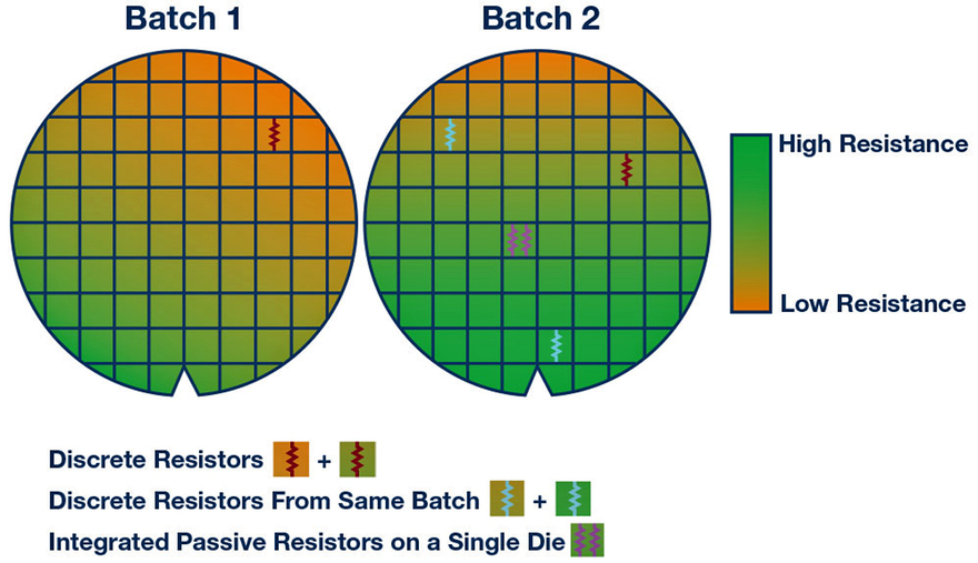
Fig. 1: Matching of discrete vs. passive resistors
The individual components within integrated passives are placed closely together (within microns in fact) and, because of this, the interconnect parasitics such as trace resistance and inductance can be kept to an absolute minimum. On PCBs, interconnect parasitics can be variable due to trace tolerances and component placement tolerances. With integrated passives, interconnect tolerances and component placement tolerances are extremely tight due to the photolithographic processes employed in their manufacture. On integrated passives, not only are the parasitics very small, but the few that are there are very predictable and, hence, can be reliably accounted for.
The miniaturization of passive networks through integrated passives has the very straightforward benefit of making circuit boards smaller. This leads directly to reducing circuit board costs and to allowing more and more functionality and performance to be packed into smaller footprints. Building systems with high channel counts becomes much more practical when using integrated passives.
Another significant advantage of integrated passives is the robustness of the complete wiring network around them. Rather than needing lots of soldered connections, integrated passives are essentially forged together in one complete unit, sealed up with glass, and then further protected with a robust plastic encapsulant. Within integrated passive networks, issues with dry solder joints, corrosion, or misplaced components are not present.
An additional benefit of integrated passive networks being so well sealed up is that the number of exposed nodes in a system is much reduced. Hence, the possibility of systems being damaged by accidental shorting or electrostatic discharge (ESD) events are significantly diminished.
Maintaining and controlling the stock of components for any circuit board assembly is quite a complex task. Integrated passives having multiple passive components within one device greatly unburdens the customers’ bill of materials, which results in the cost of ownership going down. Customers receive integrated passive networks fully tested and proven good. This means that the final board build yields are improved, and this not only enables further cost savings but also enhances supply chain predictability.
Use of iPassives
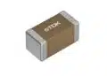
High quality passive devices have been core to the circuit performances achieved by many of ADI’s products. The integrated passives process is modular, which means that the processing steps needed to produce a certain type of passive device need only be performed if that component is needed. An iPassives network can essentially be built up with just the processing complexity required—no more and no less. As illustrated in Figure 2, there are several passive building blocks to choose from and constructing an integrated passives network can be as simple as piecing together the required components.
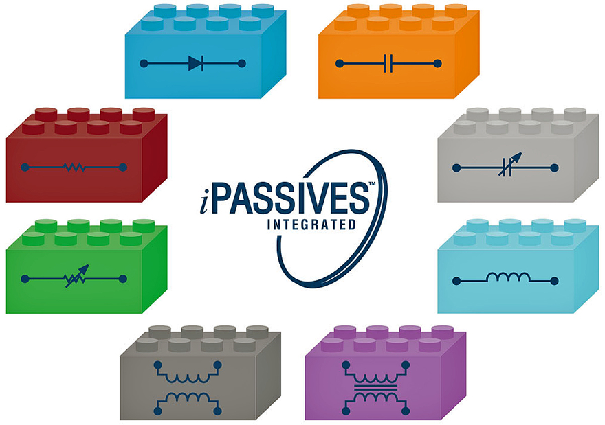
Fig. 2: Building blocks for iPassives.
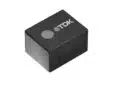
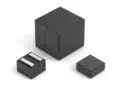
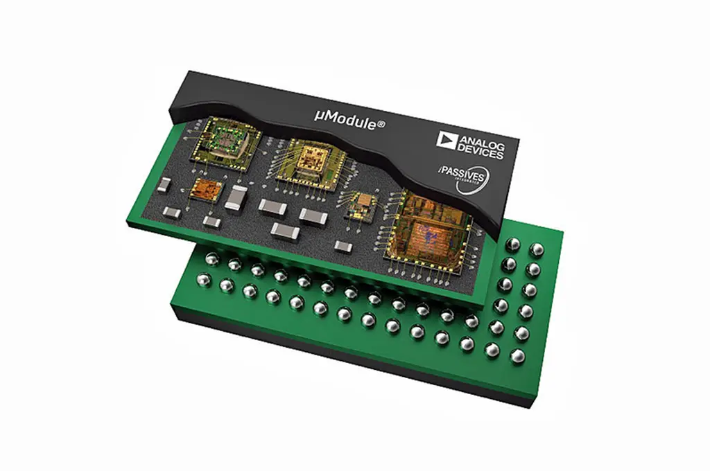
As outlined earlier, integrated passives hold many advantages over discrete passives. ADI has brought these advantages a step further by employing their use in μModule devices. These modules leverage off the capabilities of a diverse range of integrated circuits. The two μModule device examples in Figure 3 contain data converters, amplifiers, and other components, and bringing them together are passive gain and filtering networks that are built with integrated passives.
By adopting a reusability approach from a huge portfolio of field proven ICs and combining this approach with the versatility of iPassives, both the development cycle times and costs are dropping significantly. This decision offers immense benefits to customers who themselves can get to market faster and more efficiently with state-of-the-art performance.
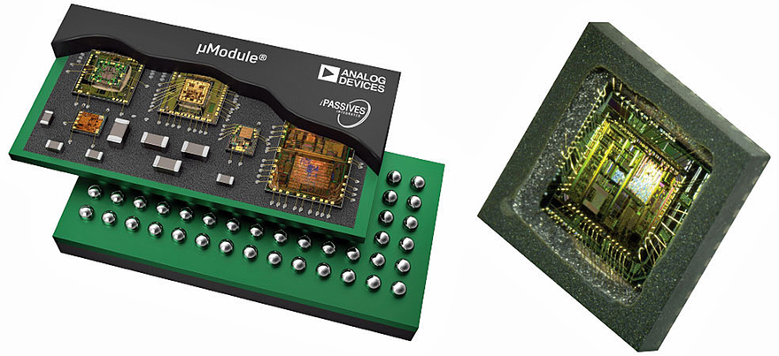
Fig. 3: μModule product examples using iPassives.
Conclusion
At first glance, the use of integrated passives may appear only incrementally more advantageous over more established approaches. The advantages, however, turn out to be significant and iPassives are redefining not just what can be done, but also what speeds, costs, and sizes are beneficial to customers.
About the authors
Mark Murphy is a product marketing engineer with Analog Devices’ Precision Converter Group in Limerick, Ireland. He holds a B.S.E.E. from Merrimack College and an M.B.A. from the University of Limerick. He can be reached at [email protected].
Pat McGuinness is a product engineer at Analog Devices with responsibility for the use of integrated passive components in system in package applications. Since joining ADI in 1994, Pat has worked on product yield improvement activities, circuit design, device modeling, and new process development. Throughout his time at ADI he has designed precision converters, switches, sensors, and passive networks. Pat received his bachelor’s degree in electrical and microelectronic engineering from University College Cork. He can be reached at [email protected].