Passive Components Blog
No Result
View All Result
  • Home
  • NewsFilter
    • All
    • Aerospace & Defence
    • Antenna
    • Applications
    • Automotive
    • Capacitors
    • Circuit Protection Devices
    • electro-mechanical news
    • Filters
    • Fuses
    • Inductors
    • Industrial
    • Integrated Passives
    • inter-connect news
    • Market & Supply Chain
    • Market Insights
    • Medical
    • Modelling and Simulation
    • New Materials & Supply
    • New Technologies
    • Non-linear Passives
    • Oscillators
    • Passive Sensors News
    • Resistors
    • RF & Microwave
    • Telecommunication
    • Weekly Digest

    Capacitances of Nonlinear MLCCs: What Datasheets Don’t Tell You

    Stackpole Releases Automotive Wide‑Termination Resistors

    How a Digital Structural Twin Can Predict Tantalum Capacitor Reliability

    SCHURTER Buys Biaodi to Boost High-Voltage Protection Portfolio

    Binder Hybrid Connector Simplifies One Cable Automation

    Tapped Inductor Buck Converter Fundamentals

    TAIYO YUDEN Releases Mini Metal Power Inductors

    Molecular Memristor Shows Record 145 kH Emergent Inductance

    Planar vs Conventional Transformer: When it Make Sense

    Trending Tags

    • Ripple Current
    • RF
    • Leakage Current
    • Tantalum vs Ceramic
    • Snubber
    • Low ESR
    • Feedthrough
    • Derating
    • Dielectric Constant
    • New Products
    • Market Reports
  • VideoFilter
    • All
    • Antenna videos
    • Capacitor videos
    • Circuit Protection Video
    • Filter videos
    • Fuse videos
    • Inductor videos
    • Inter-Connect Video
    • Non-linear passives videos
    • Oscillator videos
    • Passive sensors videos
    • Resistor videos

    Capacitances of Nonlinear MLCCs: What Datasheets Don’t Tell You

    Tapped Inductor Buck Converter Fundamentals

    Planar vs Conventional Transformer: When it Make Sense

    Modeling Fringing Field Losses in Inductors & Transformers

    Why Power Inductors Use a Ferrite Core With an Air Gap

    Transformer-Based Power-Line Harvester Magnetic Design

    Thermal Modeling of Magnetics

    Standard vs Planar LLC transformers Comparison for Battery Chargers

    How Modern Tools Model Magnetic Components for Power Electronics

    Trending Tags

    • Capacitors explained
    • Inductors explained
    • Resistors explained
    • Filters explained
    • Application Video Guidelines
    • EMC
    • New Products
    • Ripple Current
    • Simulation
    • Tantalum vs Ceramic
  • Knowledge Blog
  • DossiersNew
  • Suppliers
    • Who is Who
  • PCNS
    • PCNS 2025
    • PCNS 2023
    • PCNS 2021
    • PCNS 2019
    • PCNS 2017
  • Events
No Result
View All Result
Passive Components Blog
No Result
View All Result

Minimizing Temperature Drift in Your Current Measurement by Resistive Gain Network

14.8.2017
Reading Time: 5 mins read
A A

source: Electronic Design article

Dan Harmon | Aug 11, 2017 Use a current-sense amplifier that integrates a precisely matched, resistive gain network to minimize the temperature-drift effects of the gain error.
As more systems become electrified, thermal management has turned into one of the “hottest” issues facing designers. Using current measurements for thermal management is a leading indicator of system performance and faults, whereas simply monitoring the temperature is potentially a lagging indicator. Accurately monitoring the current consumed, especially over temperature, has become vital as designers pack more functionality into tighter areas.

RelatedPosts

Capacitances of Nonlinear MLCCs: What Datasheets Don’t Tell You

Stackpole Releases Automotive Wide‑Termination Resistors

How a Digital Structural Twin Can Predict Tantalum Capacitor Reliability

While room-temperature calibration tends to be relatively straightforward, performing multi-temperature calibration is time-consuming and costly. Identifying ways to minimize the effects of temperature on current measurements can improve system performance and minimize system design margins, as well as potentially lower the total cost of ownership (TCO).

Sources of Error in Current Measurements

As I stated in my September 2015 article, “Mitigate Error Sources to Maximize Current-Measurement Accuracy,” there are multiple contributing sources of error in current-measurement applications. In the article, I listed these sources of errors:

Amplifier-related errors:

  • Input offset voltage (VOS) and VOS drift
  • Common-mode rejection ratio (CMRR)
  • Power-supply rejection ratio (PSRR)
  • Gain error and gain drift

System errors:

  • Gain-setting network tolerance, matching, and drift
  • Printed-circuit-board (PCB) layout
  • Shunt-resistor tolerance and drift

You can see that “drift” is part of four of the seven items on both lists, which emphasizes the importance of minimizing the additional errors caused by temperature in a current-measurement implementation.

Discrete Current-Measurement Implementations

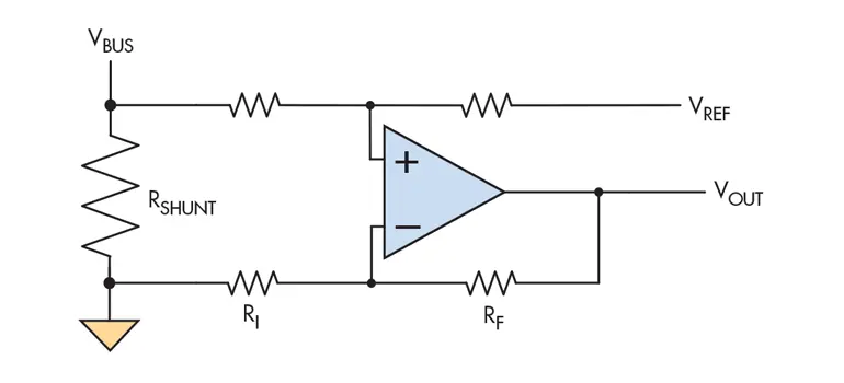
Many system designers choose a discrete amplifier and external gain network for their low-side current-measurement applications because it’s viewed as a low-cost alternative. There are two options when using a discrete circuit for low-side current sensing: a single-ended or differential configuration. Figure 1 shows the latter.

 1. This basic differential amplifier configuration is used for current measurement.

In either configuration, the gain of the system is defined as G = RF/RI. The worst-case initial (or room-temperature) gain error is simply the tolerance of the discrete gain resistors. Assuming an application with a gain of 20, where RF = 100 kΩ and RI = 5 kΩ, Table 1 reveals how that looks for different resistor tolerances.

To understand the effects of temperature, let’s assume the same gain implementation with nominal resistor values and then apply various standard temperature coefficients (tempcos). Tempcos are usually specified in terms of parts per million per degree Celsius (ppm/°C). To get from ppm to a percentage, simply divide by 10,000. Table 2 shows the calculation results for a variety of resistor tempcos.

The issue here is that the drift could be in opposite directions and different for each resistor, which means minimizing these temperature effects in gain errors requires multipoint calibration (as well as temperature monitoring) to enable temperature compensation in the system management controller. The additional circuitry and resources (calibration means people and time!) can significantly drive up the TCO. Plus, as the tempcos drop, the resistor becomes more expensive, and in turn drives up the TCO.

Calibration

As I mentioned, performing system calibration can minimize (or even eliminate) initial errors. Typical calibration occurs at the total system level and involves two-point calibration. Performing two-point calibration enables you to minimize the error at both low current levels (due to the offset of the system), as well as at higher current levels where gain error is the primary error source.

A video training series from Texas Instruments titled “Getting Started with Current Sense Amplifiers,” beginning with session 2.1, discusses this topic in detail. Equation 1 describes the transfer function of the system:
VOUT = (IL × RSHUNT × G) + VOFFSET               (1)

The intent of calibration is to identify the factors needed to correct for the amplifier’s offset voltage (VOFFSET), the gain error of the network (G), and the shunt resistor error (RSHUNT). Applying zero current calculates the necessary offset correction. Using a current close to the nominal load will calculate the total gain correction factor, accounting for both the shunt tolerance and amplifier gain network.

Minimizing the offset error is very straightforward—choose an amplifier with low VOS and low VOS drift. You will have to make a tradeoff between performance and cost. As discussed above, trying to perform two-point calibration at multiple temperatures to calculate the drift component of the offset error is costly and time-consuming.

Current-Sense Amps Integrate Precision Matched Gain Networks

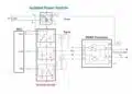
Current-sense amplifiers are specialized integrated circuits designed specifically to measure current. As shown in Figure 2, these amplifiers have four fundamental benefits compared to a discrete implementation.

2. A current-sense amplifier offers several key benefits over a discrete current-sense implementation.

The benefit of the precision, matched gain-resistor network really manifests itself in how the gain error changes over temperature. The way the resistors are designed and fabricated on-chip enables near-perfect matching of both the initial error as well as the temperature drift. The absolute accuracy of the resistors isn’t a factor in minimizing gain error; what’s critical is how well they’re matched. If both RF and RI are off by 10% in the same direction (either plus or minus), then the ratio remains ideal and the gain error is zero.

3. This part of Texas Instruments’ INA180 product datasheet electrical specifications table shows offset and offset drift.
When a current-sense amplifier specifies a room temperature gain error of 1%, for instance, in Texas Instruments’ INA180 datasheet (Fig. 3), it’s actually an indicator of how well-matched the resistors are opposed to the external gain network, where 1% resistors result in ±2% error.

4. The plot compares approximate measurement error over temperature between a current-sense amplifier with 20-ppm/°C drift and a discrete implementation using a gain network with 50-ppm/°C resistors.

The drift is also typically low on the integrated resistors—20 ppm/°C in the case of the INA180, which minimizes the effect of temperature drift on the total error. Figure 4 approximates the impact on error for two different amplifier arrangements over temperature. For this comparison, make the following assumptions:

  • An ideal 200-mΩ shunt with 0% error and no drift.
  • Room-temperature calibration to eliminate the initial offset and gain network errors.
  • Offset drift of 5 µV/°C for both configurations.
  • Configuration No. 1 uses an external gain network of 20 V/V with a 50 ppm/°C gain network.
  • Configuration No. 2 is a current-sense amplifier with matched resistors configured for a gain of 20 V/V and 20 ppm/°C drift.

Summary

Maximizing accuracy in current measurements over temperature is critical in many applications. While room-temperature calibration is relatively straightforward, performing multi-temperature calibration is time-consuming and expensive. Using a current-sense amplifier that integrates a precisely matched, resistive gain network will minimize the temperature-drift effects of the gain error.

Implementing a low-drift amplifier architecture allows you to minimize the offset error over temperature. On that front, Texas Instruments has developed zero-drift current-sense amplifiers, including the INA180 and INA181, that enable high initial room-temperature accuracy while minimizing the effects of temperature.

Related

Recent Posts

Stackpole Releases Automotive Wide‑Termination Resistors

14.5.2026
4

Molecular Memristor Shows Record 145 kH Emergent Inductance

12.5.2026
18

Stackpole Expanded its AlN Thick Film Chip Resistors

6.5.2026
23

Modelithics Releases COMPLETE v26.1 for Keysight ADS

23.4.2026
24

April 2026 Interconnect, Passives and Electromechanical Components Market Insights

22.4.2026
144

ECIA March 2026 Industry Pulse Points to Best Sales Climate in Five Years

13.4.2026
85

March 2026 Interconnect, Passives and Electromechanical Components Market Insights

2.4.2026
140

APEC 2026 Power Electronics Trends and Implications for Passive Components

1.4.2026
199

Indias ECMS Wave Brings New Capacity For Passive Components Manufacturing in India

31.3.2026
72

Upcoming Events

May 19
16:00 - 17:00 CEST

Designing Qi2 Wireless Power Systems: Practical Development and EMC Optimization

Jun 2
16:00 - 17:00 CEST

Calculation, Simulation and Measurement of 800V EMC Filters

Jun 16
16:00 - 17:00 CEST

EMC with EMC – EMC‑compliant design with electromechanical connectors

View Calendar

Popular Posts

  • Buck Converter Design and Calculation

    0 shares
    Share 0 Tweet 0
  • Boost Converter Design and Calculation

    0 shares
    Share 0 Tweet 0
  • Flyback Converter Design and Calculation

    0 shares
    Share 0 Tweet 0
  • LLC Resonant Converter Design and Calculation

    0 shares
    Share 0 Tweet 0
  • MLCC and Ceramic Capacitors

    0 shares
    Share 0 Tweet 0
  • Dual Active Bridge (DAB) Topology

    0 shares
    Share 0 Tweet 0
  • Capacitor Charging and Discharging

    0 shares
    Share 0 Tweet 0
  • What Electronics Engineer Needs to Know About Passive Low Pass Filters

    0 shares
    Share 0 Tweet 0
  • Ripple Current and its Effects on the Performance of Capacitors

    3 shares
    Share 3 Tweet 0
  • Samsung Electro-Mechanics Releases High-Capacitance MLCCs for AI Server Applications

    0 shares
    Share 0 Tweet 0

Newsletter Subscription


Passive Components Blog

© EPCI - Leading Passive Components Educational and Information Site

  • Home
  • Privacy Policy
  • EPCI Membership & Advertisement
  • About

No Result
View All Result
  • Home
  • Knowledge Blog
  • PCNS

© EPCI - Leading Passive Components Educational and Information Site

This website uses cookies. By continuing to use this website you are giving consent to cookies being used. Visit our Privacy and Cookie Policy.
Go to mobile version