• Latest
  • Trending
  • All
  • Capacitors
  • Resistors
  • Inductors
  • Filters
  • Fuses
  • Non-linear Passives
  • Applications
  • Integrated Passives
  • Oscillators
  • Passive Sensors
  • New Technologies
  • Aerospace & Defence
  • Automotive
  • Industrial
  • Market & Supply Chain
  • Medical
  • RF & Microwave
  • Telecommunication

Multilayer Chip Capacitors Visual Standards

8.10.2019

Examining the Influence of ESR and Ripple Current on Selecting the Suitable Capacitor

21.3.2023

SABIC Validates its 150°C Film Foil to Enable Adoption of Film Capacitors in SIC Power Modules

20.3.2023

Outlook of Passive Electronic Components Market for Oil & Gas Electronics in 2023

20.3.2023

Flying Capacitors Explained

17.3.2023

TDK Introduces Compact High-Current Chokes for Automotive and Industrial Applications

16.3.2023

ECIA NA February 2023 Electronic Components Sales Confirms Growth Trend

16.3.2023
  • Home
  • Privacy Policy
  • EPCI Membership & Advertisement
  • About
No Result
View All Result
NEWSLETTER
Passive Components Blog
  • Home
  • NewsFilter
    • All
    • Aerospace & Defence
    • Antenna
    • Applications
    • Automotive
    • Capacitors
    • Circuit Protection Devices
    • Filters
    • Fuses
    • Inductors
    • Industrial
    • Integrated Passives
    • Market & Supply Chain
    • Medical
    • New Materials & Supply
    • New Technologies
    • Non-linear Passives
    • Oscillators
    • Passive Sensors
    • Resistors
    • RF & Microwave
    • Telecommunication

    Examining the Influence of ESR and Ripple Current on Selecting the Suitable Capacitor

    SABIC Validates its 150°C Film Foil to Enable Adoption of Film Capacitors in SIC Power Modules

    Outlook of Passive Electronic Components Market for Oil & Gas Electronics in 2023

    Flying Capacitors Explained

    TDK Introduces Compact High-Current Chokes for Automotive and Industrial Applications

    ECIA NA February 2023 Electronic Components Sales Confirms Growth Trend

    Investigating Modeling Techniques of Class II Ceramic Capacitors Losses for High Voltage and Current Applications

    TDK Extends Range of Industrial Single Pair Ethernet (SPE) Inductors

    Premo Unveils New series of 11kW 3-Phase On-Board Charger Transformers

    Trending Tags

    • Ripple Current
    • RF
    • Leakage Current
    • Tantalum vs Ceramic
    • Snubber
    • Low ESR
    • Feedthrough
    • Derating
    • Dielectric Constant
    • New Products
    • Market Reports
  • VideoFilter
    • All
    • Antenna videos
    • Capacitor videos
    • Filter videos
    • Fuse videos
    • Inductor videos
    • Non-linear passives videos
    • Oscillator videos
    • Passive sensors videos
    • Resistor videos
    • Sensors

    Investigating Modeling Techniques of Class II Ceramic Capacitors Losses for High Voltage and Current Applications

    Understanding Basics of Current Sense Resistors

    What Decoupling Capacitor Value To Use And Where To Place Them

    How to Measure Rated Current on Power Inductors

    LTspice Simulation of a Spark-Gap Circuit Protection Surge Arrester

    Approximate Inductor Design Using Two Alternative Cores

    1kW Phase Shift Full Bridge Converter Design and Simulation

    Multiphase Buck Trans-Inductor Voltage Regulator (TLVR) Explained

    Smart Power Distribution Unit Architecture and Inductor Losses

    Trending Tags

    • Capacitors explained
    • Inductors explained
    • Resistors explained
    • Filters explained
    • Application Video Guidelines
    • EMC
    • New Products
    • Ripple Current
    • Simulation
    • Tantalum vs Ceramic
  • Knowledge Blog
  • Suppliers
    • Preferred Suppliers
    • Who is Who
  • Events
No Result
View All Result
Passive Components Blog
No Result
View All Result

Multilayer Chip Capacitors Visual Standards

8.10.2019
Reading Time: 5 mins read
0 0
0
SHARES
1.5k
VIEWS

Source: Knowles Capacitors blog

Knowles Capacitors explains the ins and outs of chips capacitors – their properties, product classifications, test standards, and use cases. In the next article, manufacturers’ MLCC chip visual standards are explained.

RelatedPosts

Examining the Influence of ESR and Ripple Current on Selecting the Suitable Capacitor

SABIC Validates its 150°C Film Foil to Enable Adoption of Film Capacitors in SIC Power Modules

Outlook of Passive Electronic Components Market for Oil & Gas Electronics in 2023

External Visual Standards

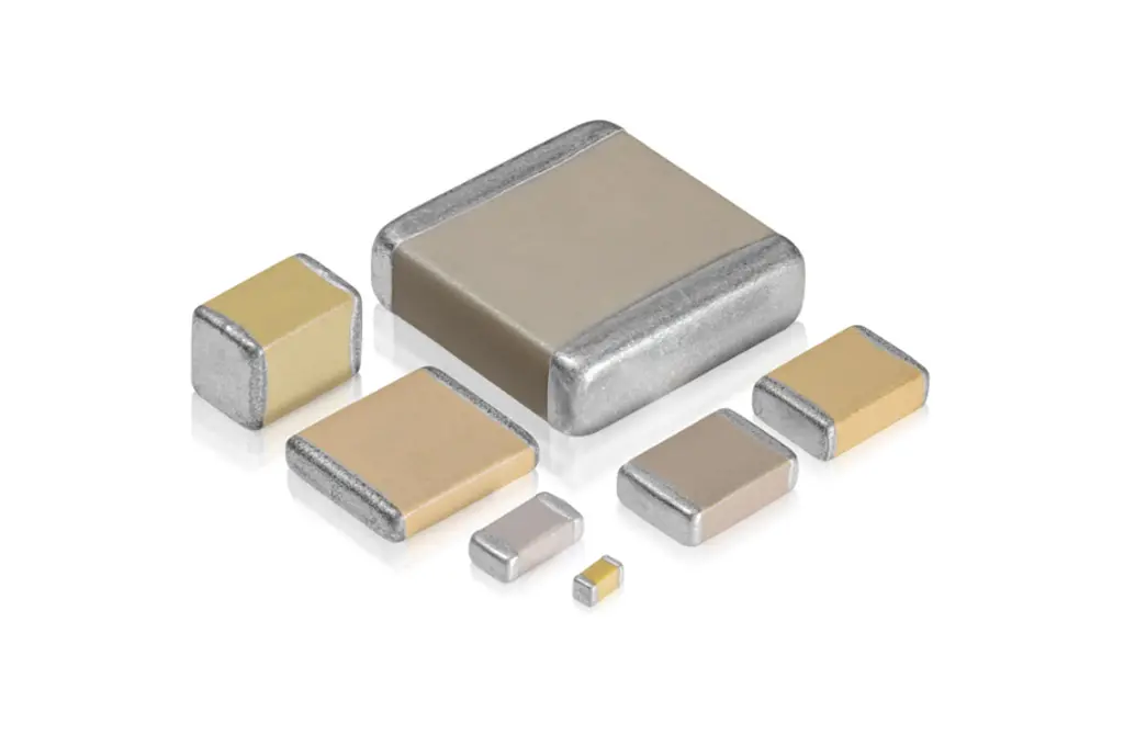
Multilayer ceramic capacitors (MLCCs) must possess fine workmanship and physical integrity, so visual inspection of the product is performed at 20X magnification to check for defects in the capacitor body and end metallization. Visual standards are detailed in MIL-C-123B, Appendix C, and manufacturers typically inspect only sample quantities in accordance with MIL STD 105, Level II, 0.65. Acceptance or rejection of standard production lots is based on various defective criteria, as listed in Table 1 and depicted in Figure 1.

 Table 1. Typical criteria for visual defects

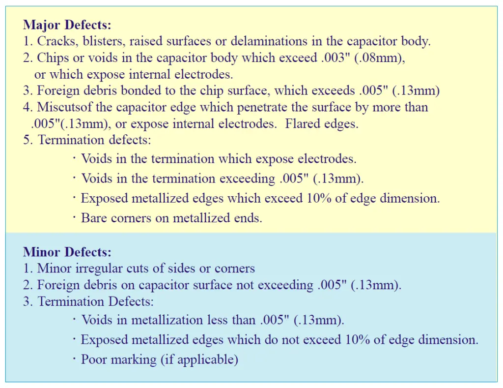
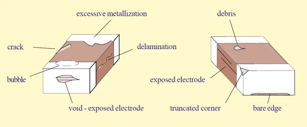
 Figure 1. Visual defects

Internal Microstructure Standards

In addition to the external visual characteristics, quality standards for internal microstructure of the chip capacitor are also applicable, as viewed on polished cross sections of capacitor samples. Units are sectioned along the long and short dimension of the capacitor to provide two edge views of the internal electrodes and terminals.

Although any degree of internal defect is considered undesirable, the fact remains that these types of defects can occur occasionally in different degrees of severity. Typically, delaminations, internal voids, cracks, and other irregularities (see in Figure 2) are classified based on their severity and are considered to constitute defects if they exceed the criteria based on EIA 469.

Delaminations

A delamination is a separation of the structural layers of the capacitor, in the form of a planar cavity, between the electrode and ceramic or within the dielectric itself. Any delamination which can be considered to be detrimental to the electrical and mechanical integrity of the capacitor is classified as a defect, and generally involves the following:

  • Any delamination in the active (electrode overlap) area, longer than 20% of the electrode length, or exceeding .010″ (.254 mm), whichever is greater
  • Any delamination greater than .005″ (.127 mm), located within the electrode overlap area, and associated with displacement of adjacent electrodes and reduction of these dielectric layers by more than 50% of their thickness
  • A delamination which exceeds 50% of the margin between the termination and electrodes of opposite polarity
  • Two or more delaminations exceeding .010″ which overlap each other in the active electrode area, in adjacent layers

Voids

Any void which can be considered detrimental to the electrical and physical integrity of the capacitor is classified as a defect, and generally involves the following:

  • Any void between electrodes of opposite polarity, which reduces the dielectric thickness by more than 50%
  • Any void in the cover plate of the capacitor which reduces the cover thickness to less than .003″ (.076 mm), or less than the active dielectric thickness
  • A void or bubble in the termination, not contacting the dielectric surface, which exceeds 30% of the chip end dimension
  • A void or bubble in the termination, contacting the dielectric, which exceeds .020″ (.508 mm)

Cracks

Any crack which can be considered detrimental to the electrical and physical integrity of the capacitor is classified as a defect, and generally involves the following:

  • Any crack connecting any two electrodes
  • Any crack connecting an electrode to any exterior surface of the chip, or to a termination
  • Cracks extending from the termination metal band into the interior of the chip (also known as termination stress cracks)

Non-Uniformities

Irregularities in the construction of the chip capacitor do not necessarily affect the mechanical or electrical integrity of the device, but may be of concern in high reliability applications. The following is a compilation of structural irregularities according to the EIA 469:

  • A side or end margin of dimension less than .003″ (.076 mm) between 90% or more of the electrodes and the exterior dielectric surface
  • Ceramic cover plate thickness which is less than the dielectric thickness between adjacent electrodes
  • Variations in the active dielectric layers which result in areas with less than 50% of the nominal dielectric thickness
  • Thick electrode depositions, exceeding 2.5 times the average electrode thickness, and extending over 50% of the electrode length
  • Thick electrode deposition, extending over .005″ (.127 mm), which also reduces the adjacent dielectric layer thickness by more than 30%

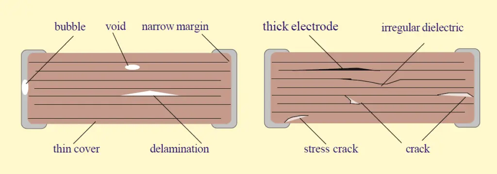
Figure 2. Microstructure defects

Sample Preparation Defects

A variety of imperfections observed on sectioned specimens can arise due to the method of sample preparation and must be identified (so as to preclude erroneous interpretation of results). Subtle observations and precautions can be followed to positively segregate preparation problems from actual defects. First, it is essential that the specimen be observed, prior to mounting in a section, to determine if any obvious mechanical flaws are present. Usually this is accompanied by inspection of basic electrical properties. Secondly, units must be rigidly encapsulated with non-shrinking (and hence stress-free) resin, followed by grinding and polishing with fine grit abrasives under controlled pressure to avoid cracking. Sections must be polished to remove all vestiges of the rough cuts used to reduce the specimen and then cleaned thoroughly before observation. This procedure will minimize the occurrence of most sectioning-induced defects (depicted in Figure 3).

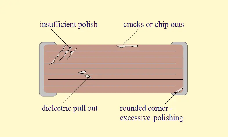
Figure 3. Sample preparation defects

The following criteria are used to attribute defects to sectioning methods:

  • Void defects form linear patterns,e. they are induced by grit pulling material out of the ceramic during grinding, hence more polishing is required. Note that voids forming a line parallel to the layered structure of the device, a so-called “knit line,” may not fall into this category.
  • Large voids are present, with virtually no distortion of the electrode pattern or of adjacent dielectric layers. The correctness of the structure around these voids is indicative as to their absence in the original unsectioned unit; thermal processing would otherwise result in collapse of the electrode and/ or distortion of layers around these voids. Such defects are caused by excessive pullout during grinding, particularly in the area between electrode layers, where there is minimal dielectric layer to layer bonding.
  • Units exhibit cover sheet cracks and/or separation of the ceramic cover sheet from the electrode array, yet these were not evident on usual examination of the device prior to sectioning. These defects arise due to insufficient support in the encapsulant and/or excessive grinding methods. Such cracks may also appear parallel to the end terminations, as the termination to ceramic interface is mechanically weaker. Measurements of capacitance, dissipation factor (DF), insulation resistance, and termination pull strength can be used to confirm the absence of this defect in unsectioned product.
  • Excessive polishing will round corners and edges of the section, resulting in depth of field distortions on observation, as well as difficulty with illumination. “Defects” which appear under these conditions may be nonexistent and should be disregarded.

Evaluation of visual and microstructure quality of chip capacitors is very subjective, and difficulties arise in correlating opinions between observers, especially when considering the minor category of defects described above. In addition, dissimilar images can occur when viewing product under differing light sources on a microscope. (Fluorescent lighting has been found to be superior over incandescent light in highlighting defects.) The acceptance or rejection of capacitors with any visual or microstructure defects is usually specified or determined by the chip user, based on the application of the product. High reliability or high voltage units must meet the most stringent standards.

Related Posts

Capacitors

Examining the Influence of ESR and Ripple Current on Selecting the Suitable Capacitor

21.3.2023
48
Capacitors

SABIC Validates its 150°C Film Foil to Enable Adoption of Film Capacitors in SIC Power Modules

20.3.2023
16
Market & Supply Chain

Outlook of Passive Electronic Components Market for Oil & Gas Electronics in 2023

20.3.2023
15

Upcoming Events

Mar 19
March 19 - March 23

APEC 2023

Mar 22
14:00 - 15:00 CET

Parasitic Components in Power Converters – Fundamentals and Measurements Rohde & Schwarz Webinar

Apr 3
April 3 @ 12:00 - April 4 @ 14:00 CEST

Microelectronic Packaging Failure Modes and Analysis

View Calendar

Popular Posts

  • What is a Dielectric Constant of Plastic Materials ?

    4 shares
    Share 4 Tweet 0
  • Ripple Current and its Effects on the Performance of Capacitors

    3 shares
    Share 3 Tweet 0
  • Capacitor Selection for Coupling and Decoupling Applications

    28 shares
    Share 28 Tweet 0
  • Understanding High-Precision Resistor Temperature Coefficient of Resistance

    0 shares
    Share 0 Tweet 0
  • Leakage Current Characteristics of Capacitors

    0 shares
    Share 0 Tweet 0
  • How to Choose the Right Inductor for DC-DC Buck Applications

    0 shares
    Share 0 Tweet 0
  • Examining the Influence of ESR and Ripple Current on Selecting the Suitable Capacitor

    0 shares
    Share 0 Tweet 0
  • Why Low ESR Matters in Capacitor Design

    0 shares
    Share 0 Tweet 0

Newsletter Subscription


PCNS Call for Papers !

Archive

2022
2021
2020
2019
2018
2017

Symposium

Passive Components Networking Symposium

Passives e-Learning

Knowledge Blog

  • Home
  • Privacy Policy
  • EPCI Membership & Advertisement
  • About

© EPCI - Premium Passive Components Educational and Information Site

No Result
View All Result
  • Home
  • News
  • Video
  • Knowledge Blog
  • Preferred Suppliers
  • Events

© EPCI - Premium Passive Components Educational and Information Site

Welcome Back!

Login to your account below

Forgotten Password?

Retrieve your password

Please enter your username or email address to reset your password.

Log In
This website uses cookies. By continuing to use this website you are giving consent to cookies being used. Visit our Privacy and Cookie Policy.