Passive Components Blog
No Result
View All Result
  • Home
  • NewsFilter
    • All
    • Aerospace & Defence
    • Antenna
    • Applications
    • Automotive
    • Capacitors
    • Circuit Protection Devices
    • electro-mechanical news
    • Filters
    • Fuses
    • Inductors
    • Industrial
    • Integrated Passives
    • inter-connect news
    • Market & Supply Chain
    • Market Insights
    • Medical
    • Modelling and Simulation
    • New Materials & Supply
    • New Technologies
    • Non-linear Passives
    • Oscillators
    • Passive Sensors News
    • Resistors
    • RF & Microwave
    • Telecommunication
    • Weekly Digest

    High-Q RF & Microwave MLCCs: A Cross-Vendor Benchmark

    Molex Unveils Automotive Ethernet Connectors for Next‑Gen SDV Architectures

    TAIYO YUDEN Introduced Hybrid Aluminum Capacitors for 48V Automotive Power Supplies

    ECIA Industry Pulse June 2026 Reaches Five‑Year High

    YAGEO Announces July 2026 Capacitor Price Increase

    YAGEO Presents Single-Phase Common Mode Chokes for Industrial EMI Suppression

    Enabling the 800 V AI Server Era: How C0G High-Voltage MLCC Supports Next-Generation Power Architectures

    binder Prints Electronics on 3D Components Connector Surface

    Vishay Introduces SMD Polymer PTC Thermistors for Fast Resettable Overcurrent Protection

    Trending Tags

    • Ripple Current
    • RF
    • Leakage Current
    • Tantalum vs Ceramic
    • Snubber
    • Low ESR
    • Feedthrough
    • Derating
    • Dielectric Constant
    • New Products
    • Market Reports
  • VideoFilter
    • All
    • Antenna videos
    • Capacitor videos
    • Circuit Protection Video
    • Filter videos
    • Fuse videos
    • Inductor videos
    • Inter-Connect Video
    • Non-linear passives videos
    • Oscillator videos
    • Passive sensors videos
    • Resistor videos

    KYOCERA AVX Presents Antenna Integrator Studio Tutorial for Antenna Placement and RF Design

    Power Design Simulation Tools for Faster Inductor Selection and Loss Optimization

    EMC‑Compliant PCB and Connector Design Guidelines

    Why Isolated DC/DC Power Supplies Fail Late, Würth Elektronik Podcast

    Designing 800 V DC EMC Filters: Calculation, Simulation and Measurement

    Current Sense Transformer Datasheet and Design‑in Guide

    Designing a USB Type‑C Flyback Planar Transformer with Frenetic’s Planar Tool

    Magnetics Design in High‑Frequency GaN Converters

    Qi2 Wireless Charging: Inductors, Capacitors and EMC Filters

    Trending Tags

    • Capacitors explained
    • Inductors explained
    • Resistors explained
    • Filters explained
    • Application Video Guidelines
    • EMC
    • New Products
    • Ripple Current
    • Simulation
    • Tantalum vs Ceramic
  • Knowledge Blog
  • DossiersNew
  • Suppliers
    • Who is Who
  • PCNS
    • PCNS 2025
    • PCNS 2023
    • PCNS 2021
    • PCNS 2019
    • PCNS 2017
  • Events
No Result
View All Result
Passive Components Blog
No Result
View All Result

Reduce Harmonic Distortion by Decoupling Capacitor

15.2.2021
Reading Time: 7 mins read
A A

Learn how to reduce second harmonic distortion by following some guidelines for placing decoupling capacitors in your PCB layout in article from Steve Araras published by All About Circuits.

In this article, we’ll see that, without proper decoupling, we cannot extract the maximum linearity performance from a high-speed op-amp. In addition, we’ll discuss that simply rearranging a decoupling capacitor can affect the distortion performance of a high-speed amplification stage. 

RelatedPosts

High-Q RF & Microwave MLCCs: A Cross-Vendor Benchmark

Molex Unveils Automotive Ethernet Connectors for Next‑Gen SDV Architectures

TAIYO YUDEN Introduced Hybrid Aluminum Capacitors for 48V Automotive Power Supplies

Poor Capacitor Decoupling Can Increase Distortion

The power and ground conductors of a PCB do exhibit some inductance. This inductance can cause issues if we attempt to provide the high-frequency currents of a device directly through the power and ground conductors.

Recall that the voltage drop that appears across an inductor is proportional to the rate of change of current. Hence, at higher frequencies, a relatively larger voltage drop will appear across the power and ground conductors and we won’t be able to deliver a constant supply voltage to the IC. 

With a high-speed op-amp, the variations on the supply voltage will be signal-dependent and consequently, the linearity performance will be significantly degraded.

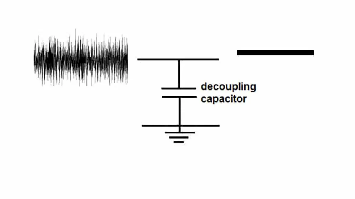
To address this issue, we place decoupling capacitors close to the op-amp supply pins. Acting as a source of charge, decoupling capacitors provide the high-frequency currents and significantly reduce the variations on the supply voltage. The following figure shows the frequency content at the output of the AD9631 op-amp driving a 100Ω load.

Figure 1. The spectral output of the AD9631 op amp with proper decoupling (left) and no decoupling (right). Image courtesy of Analog Devices.

As you can see, with proper decoupling, the distortion components are dramatically reduced.

Keep the Capacitor Ground Terminal Away from the Op-Amp Inputs

PCB layout is a key factor when optimizing the distortion performance of a high-speed board. Consider the layout examples shown below for a non-inverting amplification stage that uses an op-amp in an SOIC package.

In these examples, all components are placed on the top side of the board and only the bypass capacitor of the positive rail (Cbypass1) is on the bottom side. We assume that the board has a dedicated ground plane and the vias, represented by the green circles, connect a trace or pad to this ground plane. 

Figure 2. Two circuit diagrams with differing placement of the bypass capacitor of the negative rail.

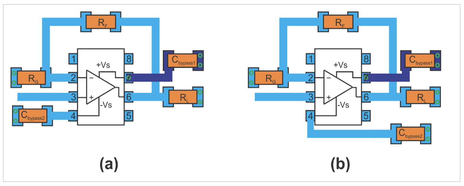
As you can see, the two layouts are exactly the same except for the placement of the bypass capacitor of the negative rail (Cbypass2). While the layout on the left places the ground side of Cbypass2 close to the op-amp inputs, the layout on the right side attempts to keep this terminal close to the load and away from the op-amp inputs.

The layout in Figure 2(b) can achieve a better distortion performance. 

Pay Careful Attention to the Return Current Path

To understand why the layout in Figure 2(b) exhibits a lower distortion, consider the return current flowing through the ground plane when the signal applied to the load has a negative polarity, i.e., Cbypass2 is supplying the load current.

When the output signal polarity is negative, the current drawn from the load flows through the top layer trace and the op-amp circuitry as shown by the blue arrows in Figure 3. 

Figure 3. The same diagrams as in Figure 2, but showing the current flow with blue arrows.

We know that the high-frequency return current flows directly underneath the signal trace to minimize the loop area. Hence, the return current of the layout in Figure 3(a) should follow a path similar to that shown by the red line.

However, it is important to note that, although most of the return current flows directly underneath the signal trace, it still can spread out slightly on the ground plane as shown in Figure 4. 

Figure 4. Distribution of high-frequency return current. Image courtesy of Segera Davies.

Therefore, with the layout in Figure 3(a), the return current can perturb the voltage at the op-amp inputs. The error signal coupled to the op-amp inputs will be signal-dependent and consequently, will cause distortion at the op-amp output. Since the signal-dependent error voltage appears only during one polarity of the output voltage (the negative polarity), it will mainly increase the second harmonic distortion.

What path the return current will choose on the ground plane in Figure 3(b)?

Again, the path directly underneath the signal trace (below the blue arrows) will offer the lowest possible inductance. However, in this case, the ground side of the bypass cap is very close to the ground terminal of the load. Hence, the path shown by the red arrow in 3(a) can offer a very small resistance compared to that of the path of the least inductance. In fact, the return current will choose the path of least impedance (both the path inductance and resistance should be considered).

To determine the exact distribution of the return current, we’ll need simulation tools; however, we can deduce that a portion of the return current will flow around the red arrow and a relatively smaller current will flow underneath the blue arrows. With a relatively smaller current flowing underneath the signal trace, we can expect to have a “quieter” ground below sensitive nodes of the circuit (around the op-amp inputs). 

Keeping the ground side of the bypass caps away from the op-amp inputs is an effective technique for reducing harmonic distortion and it is commonly recommended in different technical documents from different chip manufacturers.

What If the Load Is Far from the Op-Amp Output?

Let’s take a look at one more example wherein the load is located at a distance from the op-amp output as shown in Figure 5.

Figure 5. Our example op-amp circuit but with the load farther from the op-amp output.

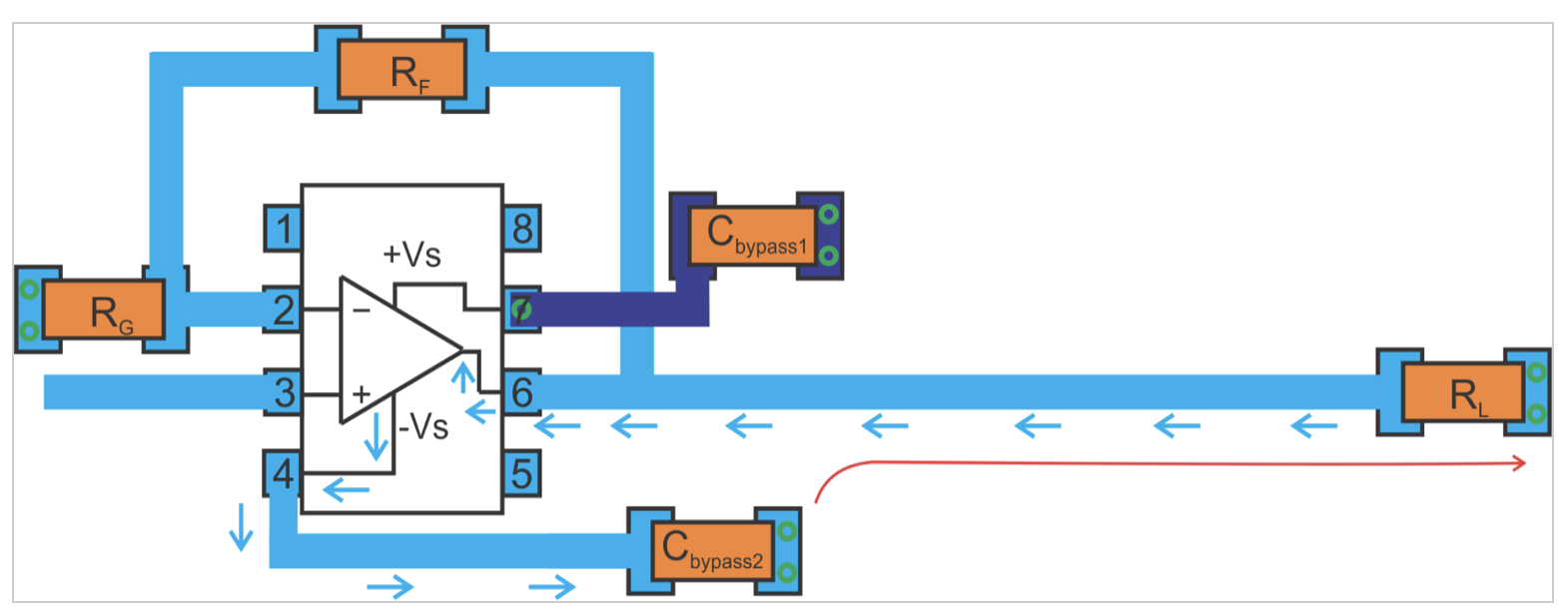
Again, we should keep the ground side of the bypass capacitor away from the op-amp inputs. The capacitor should be placed close to the op-amp power supply pin with its ground terminal close to the op-amp output.

A considerable portion of the return current should follow the low-resistance path discussed above leading to the return current path shown by the red line in the following figure.

Proper decoupling is required to extract the maximum linearity performance from a high-speed op-amp. Additionally, the ground side of the bypass capacitor should be placed close to the op-amp out and away from its inputs so that we can have a “quieter” ground under the sensitive nodes of the circuit (around the op-amp inputs).

Kemet Webinar: Decoupling and Filtering – How to Choose Capacitors for Both

Related

Source: All About Circuits

Recent Posts

High-Q RF & Microwave MLCCs: A Cross-Vendor Benchmark

2.7.2026
32

TAIYO YUDEN Introduced Hybrid Aluminum Capacitors for 48V Automotive Power Supplies

2.7.2026
21

YAGEO Announces July 2026 Capacitor Price Increase

1.7.2026
277

Enabling the 800 V AI Server Era: How C0G High-Voltage MLCC Supports Next-Generation Power Architectures

1.7.2026
77

MLCCs in the Age of AI: Q2 2026 Market Tightness

30.6.2026
231

AI Hardware Demand for Passive Components Dossier

30.6.2026
80

Power Design Simulation Tools for Faster Inductor Selection and Loss Optimization

29.6.2026
25

Skeleton Supercapacitor Achieves UL‑certified 3,500 A Peak Current for AI Data Centers

26.6.2026
64

100 V Hybrid Polymer Capacitor from VINA Enesol Targets 48–72 V Power Platforms

26.6.2026
129

Upcoming Events

Jul 14
16:00 - 17:00 CEST

EMC Design Essentials: Mastering Varistors and Common Mode Chokes

Jul 21
16:00 - 17:00 CEST

Safety by design: X and Y Interference suppression capacitors for power line filters

Jul 28
8:00 - 11:00 CEST

Post Procurement Testing of EEE Components for LEO Space Applications

View Calendar

Popular Posts

  • Boost Converter Design and Calculation

    0 shares
    Share 0 Tweet 0
  • Buck Converter Design and Calculation

    0 shares
    Share 0 Tweet 0
  • LLC Resonant Converter Design and Calculation

    0 shares
    Share 0 Tweet 0
  • Flyback Converter Design and Calculation

    0 shares
    Share 0 Tweet 0
  • MLCC and Ceramic Capacitors

    0 shares
    Share 0 Tweet 0
  • Nvidia Vera Rubin: Why One AI Rack Needs So Many More MLCC Capacitors

    0 shares
    Share 0 Tweet 0
  • Earthing Systems and IEC Classification Explained

    0 shares
    Share 0 Tweet 0
  • Dual Active Bridge (DAB) Topology

    0 shares
    Share 0 Tweet 0
  • MLCC Case Sizes Standards Explained

    0 shares
    Share 0 Tweet 0
  • SEPIC Converter Design and Calculation

    0 shares
    Share 0 Tweet 0

Newsletter Subscription


Passive Components Blog

© EPCI - Leading Passive Components Educational and Information Site

  • Home
  • Privacy Policy
  • EPCI Membership & Advertisement
  • About

No Result
View All Result
  • Home
  • Knowledge Blog
  • Dossiers
  • PCNS

© EPCI - Leading Passive Components Educational and Information Site

This website uses cookies. By continuing to use this website you are giving consent to cookies being used. Visit our Privacy and Cookie Policy.
Go to mobile version