


source: Science Daily news
February 21, 2017, Sandia National Laboratories. A new study lays down ceramic coatings kinetically at room temperature. Coating at room temperature makes microelectronics design and fabrication more flexible and could someday lead to better, less expensive microelectronics components that underpin modern technology.
Researcher Pylin Sarobol explains an elegant process for ultrafine-grained ceramic coatings in a somewhat inelegant way: sub-micron particles splatting onto a surface.
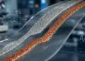
That splatting action is a key part of a Sandia National Laboratories project to lay down ceramic coatings kinetically. By making high-velocity submicron ceramic particles slam onto surfaces at room temperature, Sarobol and her colleagues avoid the high temperatures otherwise required to process ceramics like alumina and barium titanate.
Coating at room temperature makes microelectronics design and fabrication more flexible and could someday lead to better, less expensive microelectronics components that underpin modern technology. The kinetic process produces nanocrystalline films that are very strong and could be used as protective coatings against wear, corrosion, oxidation and the like.
Sarobol, who works on coatings and additive manufacturing, said it’s difficult to consolidate ceramic coatings and similar hard materials and then integrate them into devices with materials that have relatively low melting temperatures. Because ceramic components are processed at temperatures of about 1,300 degrees Fahrenheit (700 degrees Celsius) or more, it can be difficult to combine them with certain materials that have particular functions within electrical and mechanical devices. For example, current miniature waveguides require micro-machining out a tiny piece of electromagnetic material and gluing it onto another material.
“The ability to put down ceramics at room temperature means you can process ceramics and lower-melting temperature materials at the same time,” said Sarobol, who leads the project, now in its second year. “You can now put ceramics on copper, for example. Before you had to make the ceramics first, then put the copper down on it. This process is really about being able to integrate materials, especially ceramics, with other materials.”
It opens up new possibilities for fabrication — electrical circuits combining hybrid materials or tiny capacitors or sensors. “You can imagine spraying functional materials onto a circuit board rather than high-temperature processing, followed by tedious manual assembly,” Sarobol said.
Taking advantage of kinetic energy and materials properties
Rather than heat, aerosol deposition uses kinetic energy and special material properties found at micro- and nano-scales.
There’s still much to learn about the process. “We really need to spend the time to understand the process parameters, how they relate to the resulting microstructures and to the final material properties that we need,” Sarobol said. “When we think about designing a new device, we need to keep the relationship of structure-processing-properties in mind and allow ourselves time to perform the research, the optimization, and understand how we can make the properties of coatings better.”
Room-temperature microscale coatings won’t be a panacea, however, because the process produces nanocrystalline structures — not ideal for coatings for applications such as micro-actuators, micro-motors or capacitors that need large grain structure for better device function, she said.
“The aerosol-deposited coatings are made up of tiny, 20 nanometer crystals that we often call crystallites or grains,” Sarobol said. “When we heat our coatings, these tiny crystals grow and the properties change. By controlling the crystallite size, we can tune the properties in predictable ways to make more functional devices” for different applications.
Only a few of places in the world work on such room temperature, kinetic coating processes. Sarobol’s initial research came as principal investigator for a two-year project, “Room Temperature Solid-State Deposition of Ceramics,” that ended in March 2016. It led to better understanding of the basic building blocks of coatings and the scientific fundamentals behind the process.
Next comes optimizing the process, expanding the materials that can be fabricated and developing them for potential applications, which could take years.
In a nutshell, this is how it works: In aerosol deposition, a nozzle accelerates submicron particles suspended in a gas toward the surface. Particles impact and stick, building up a coating layer by layer. A key is to use submicron particles (50 times smaller than the diameter of a human hair) that allow researchers to tap into materials properties found only at small scales and activate plastic deformation in the aerosol particles. Plastic deformation, or plasticity, is a way to cause a substance to permanently change size or shape under applied stress. It’s the plasticity of submicron particles that causes consolidation of subsequent deposition layers and generates the continuous surface that layers are built upon.
Another key: deposition in a vacuum, which helps alleviate the effects of reflected gases on the flying particles. Reflection of the high-velocity carrier gas from the deposition substrate can create so-called bow shock, a gas boundary layer that’s difficult for the smallest of particles to penetrate. But in a vacuum, reflected gases are diffused so the bow shock layer is thinner. The smaller particles traveling fast have high momentum and can get through the thin bow shock layer. Without a vacuum, the bow shock layer is large and particles don’t have enough momentum to penetrate to the substrate.
Plastic deformation critical to process
Maintaining the particle kinetic energy through the bow shock layer is critical to achieve material plastic deformation, and without plastic deformation there’s no sticking and no coating.
When a particle impacts the substrate or another layer, it plastically deforms and changes shape by a process known as dislocation nucleation and slip. Sarobol’s team discovered particles have nanofractures that make them “lay down onto a substrate like splatting cookie dough, forming a pancake-shaped grain.”
The next particle that hits and deforms tamps down the original layer, creating an even tighter bond. “So you have both the materials deformation or shape change and fracturing without fragmentation, and finally the tamping from subsequent particles to help build the coating,” Sarobol said.
Those mechanisms make many layers possible, building up coatings that are tens of microns thick. “We have made nickel coatings as thick as 40 microns, and in literature I’ve seen reports of up to about 80 microns for ceramics,” Sarobol said.
Team members have successfully deposited multiple materials using the method, including copper, nickel, aluminum oxide, titanium dioxide, barium titanate and carbide compounds. Likely applications for this short list of materials alone include capacitors, resistors, inductors, electrical contacts and wear surfaces.
An enticing application specific to barium titanate films is electric field management in high-voltage systems. High-voltage capacitors, for example, are prone to failure where the dielectric material (barium titanate) meets the copper electrode and air, creating a three-material junction.
“If you spray on barium titanate at this junction, you open up the possibility of higher power capacitors,” Sarobol said. “There’s much more to do before we achieve good enough properties for that.”
Other researchers are interested in electrical contacts, protective coatings or consolidating brittle and intermetallic compounds for the first time.
The process also spans the microscale gap between two established technologies, thin films and thermal spray technology. Thin films are coating layers, ranging in size from nanometers to a few microns, that can be defined into precision electrical circuits and are patterned via photolithography techniques instead of traditional printed circuit boards. Thermal spray technology can produce coatings starting at about 50 microns up to a few centimeters.
“This can bridge that missing gap, where you can start to deposit hundreds of nanometers of materials up to a hundred microns,” Sarobol said.
Sandia National Laboratories is a multimission laboratory operated by Sandia Corporation, a wholly owned subsidiary of Lockheed Martin Corp., for the U.S. Department of Energy’s National Nuclear Security Administration. With main facilities in Albuquerque, N.M., and Livermore, Calif., Sandia has major R&D responsibilities in national security, energy and environmental technologies and economic competitiveness.
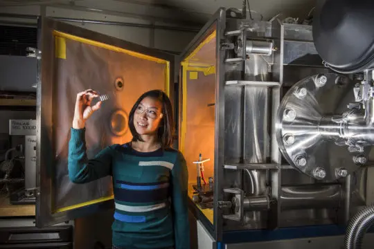
featured image: Sandia National Laboratories researcher Pylin Sarobol looks at samples of carbide coatings as she stands in front of a deposition chamber. Sarobol and colleagues are working on a process to lay down ceramic coatings kinetically, avoiding the high temperatures that otherwise would be required.
Credit: Randy Montoya