• Latest
  • Trending
  • All
  • Capacitors
  • Resistors
  • Inductors
  • Filters
  • Fuses
  • Non-linear Passives
  • Applications
  • Integrated Passives
  • Oscillators
  • Passive Sensors
  • New Technologies
  • Aerospace & Defence
  • Automotive
  • Industrial
  • Market & Supply Chain
  • Medical
  • RF & Microwave
  • Telecommunication

When are we going to print PCBs on 3D printer ourselves?

4.10.2018

Introduction of Knowles MLCCs StackiCap, its Benefits and Applications

25.5.2023

Murata Unveils Compact MLCCs with Extended Creepage Distance

25.5.2023

Properties and Characteristics of Crystal Units

24.5.2023

YAGEO Releases High Capacitance 630V NP0 MLCC for Higher Power Density and Efficiency Circuits

24.5.2023

Skeleton Acquires Former Batteries Plant to Increase Manufacturing Capacity

23.5.2023

TDK Enhances Efficiency of Materials Development Using Advanced AI

23.5.2023
  • Home
  • Privacy Policy
  • EPCI Membership & Advertisement
  • About
No Result
View All Result
NEWSLETTER
Passive Components Blog
  • Home
  • NewsFilter
    • All
    • Aerospace & Defence
    • Antenna
    • Applications
    • Automotive
    • Capacitors
    • Circuit Protection Devices
    • Filters
    • Fuses
    • Inductors
    • Industrial
    • Integrated Passives
    • Market & Supply Chain
    • Medical
    • New Materials & Supply
    • New Technologies
    • Non-linear Passives
    • Oscillators
    • Passive Sensors
    • Resistors
    • RF & Microwave
    • Telecommunication

    Introduction of Knowles MLCCs StackiCap, its Benefits and Applications

    Murata Unveils Compact MLCCs with Extended Creepage Distance

    Properties and Characteristics of Crystal Units

    YAGEO Releases High Capacitance 630V NP0 MLCC for Higher Power Density and Efficiency Circuits

    Skeleton Acquires Former Batteries Plant to Increase Manufacturing Capacity

    TDK Enhances Efficiency of Materials Development Using Advanced AI

    Transformer Optimal Operating Frequency for Phase-Shifted Full-Bridge Converter

    Vishay Unveils 120W High Energy Power Resistor

    Knowles Offers Build-to-Print Services for Thin Film Circuits

    Trending Tags

    • Ripple Current
    • RF
    • Leakage Current
    • Tantalum vs Ceramic
    • Snubber
    • Low ESR
    • Feedthrough
    • Derating
    • Dielectric Constant
    • New Products
    • Market Reports
  • VideoFilter
    • All
    • Antenna videos
    • Capacitor videos
    • Filter videos
    • Fuse videos
    • Inductor videos
    • Non-linear passives videos
    • Oscillator videos
    • Passive sensors videos
    • Resistor videos
    • Sensors

    Fast 25kW SiC EV Charger Design; OnSemi and Würth Elektronik Webinar

    PFC Inductor Magnetic Design Considerations; Frenetic Webinar

    Introduction to Capacitor Technologies; WE Webinar

    Self-Adjusting and Economical Switched Capacitor Balancer for Serially Connected Storage-Cells

    How to Design EMC Efficient Power Converter; WE Webinar

    Selecting Capacitors for High Power Buck-Booster Converters

    How to use Off-the-Shelf Transformers in Switching Power Supplies

    Simple Capacitors Pre-Charger Based on Unique ‘Floating Integrator’

    Practical LLC Transformer Design Methodology

    Trending Tags

    • Capacitors explained
    • Inductors explained
    • Resistors explained
    • Filters explained
    • Application Video Guidelines
    • EMC
    • New Products
    • Ripple Current
    • Simulation
    • Tantalum vs Ceramic
  • Knowledge Blog
  • Suppliers
    • Preferred Suppliers
    • Who is Who
  • Events
No Result
View All Result
Passive Components Blog
No Result
View All Result

When are we going to print PCBs on 3D printer ourselves?

4.10.2018
Reading Time: 6 mins read
0 0
0
SHARES
3
VIEWS

featured image: 3D printed 2-layer Arduino Board printed on the DragonFy 2020 3D Printer; image credit: Nano-dimension

Source: EPCI original article

RelatedPosts

Introduction of Knowles MLCCs StackiCap, its Benefits and Applications

Murata Unveils Compact MLCCs with Extended Creepage Distance

Properties and Characteristics of Crystal Units

by Tomas Zednicek, owner and director of European Passive Components Institute

The development of PCB 3D printers is potentially linked with a number of topics and challenges that can be closely related to passive components. The question I asked myself about 3D PCB printing capabilities was also inhibited by the current shortage of certain passive components.

The large volume manufacturers have usually a longer term contracts and negotiation power to secure its sources, thus the main shortage pain is usually with small and medium size EMS manufacturers. Hence the question is:

“Will we be able in a close future to resolve shortage of at least some passive components at small-medium volumes by direct 3D printing of PCBs?”

To get answer I decided to contact Israel company Nano-dimension that was awarded by Productronica 2017 innovation prize for its DragonFly 2020 Pro PCB 3D printer.  I was interested to find out if the PCB 3D printing process is ready to print passive components as part of its PCB printing process.  Nano-Dimension invited me and Mr.Radek Nekarda, director of Amtech, a Czech assembly equipment specialist company, to visit their technology center in Israel and meet their experts to get better understanding of the current PCB 3D printing capabilities.

The latest PCB 3D printer DragonFly 2020 Pro is the latest generation introduced to the market in Autumn 2017.

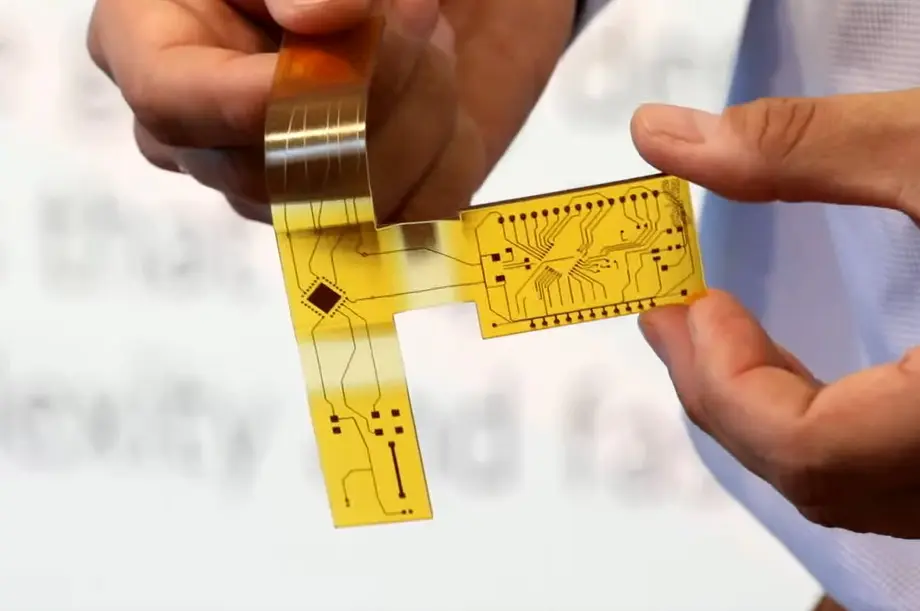
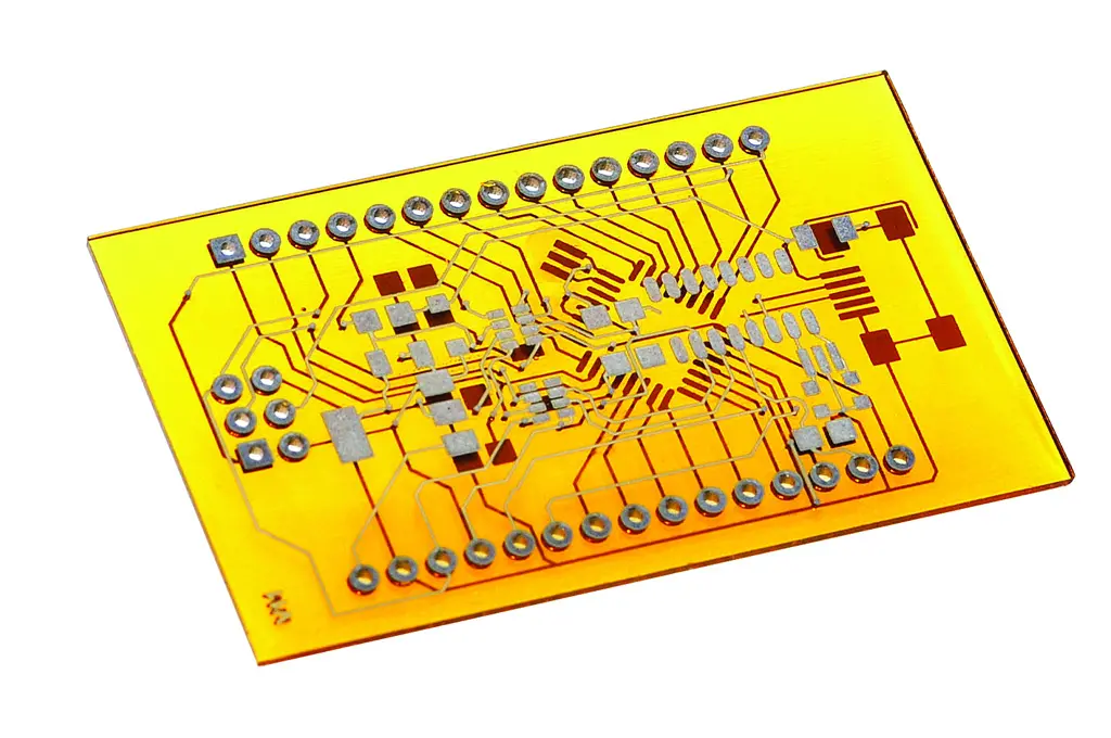
Fig. 1. and Fig.2 bottom right: PCB examples printed by DragonFly2020 Pro 3D printer; image credit: Nano-dimension

How does it work ?

The DragonFly 3D printer uses a precision additive printing process combining deposition of two types of inks – a non-conductive photo-polymer and a conductive nano-silver ink.  It‘s a full additive process, that means that both polymer and silver are step by step printed by drops and layers. The Z resolution of nano-silver ink 0.3μm and polymer dielectric 3μm is sufficient to print fine structures, conductive or insulated holes flexibly in 3D space volume.

The printed ink drop is immediately cured, but each material is cured differently. The photo-polymer by UV light and the nano-silver is sintered by heat. The silver sintering is necessary to melt the nano-particles and thus make stable PCB electrical and mechanical properties.

The printed PCB can be assembled by automatic pick and place process, however the current limitation is in temperature stress and the PCB can be mounted using low temperature soldering process only around 140-150°C. The electrical dielectric features are close to FR4 PCB, mechanical are little worse, nevertheless still sufficient for prototyping work as the main target use of the 3D printer.

The printing process can be stopped anytime, discrete components can be inserted and process continued. This gives another potential direction of use of embedded components – not only passives.

The key advantage is that you have a full flexibility for your imagination to realize 3D structures in a bulk volume of PCB. Thus you can design a structure that is difficult or impossible to make using conventional techniques such as a spiral coil from bottom PCB layer through all layers to the top. This can be of interest specifically for RF ID or antenna designers with unlimited shape modifications.

The DragonFly 2020 Pro accepts standard Gerber files, prepared by EDA PCB design softwares. 3D structures can be designed by SolidWorks with available plug-in that processes it and sends it directly to the 3D printer.

I asked Mr. Simon Fried, Nano-dimension president of North America and co-founder a few questions:

Q1: What technology evolution / revolution was necessary to bring the 3D PCB printing from laboratory to industrial ready solution?

It is a complex multidisciplinary challenge that integrates advanced materials with sophisticated algorithms and high precision hardware. The ability to print and process multiple materials (polymer and metal) at the same is a significant hurdle to overcome when replacing traditional PCB processes with what is the beginning of the era of a ‘factory in a box’.

Q2: What are the current applications / industry with highest interest / potential use of Dragonfly?

R&D groups both academia and corporate that wish to explore geometries that are difficult of impossible with traditional methods, strong interest from the defence community as they can develop products in secrecy in-house, across sectors there is constant pressure to work faster and to have more flexible workflows which AM can also facilitate. Antennas are also an area generating much interest because of the ease with which designs can now be tested with the DragonFly Pro.

Q3: in what directions we can expect the next advances of 3D PCB printing?

This is a technology that will not be going away. A wider set of materials, larger/faster systems, integrated assembly will ultimately enable highly complex electro-mechanical objects to be fully made and assembled. This means the ability to work in secret, to be able to customize, to distribute manufacturing locations, to change logistical procedures.

There is currently a situation where companies such as Siemens and Dassault are begining to bridge the gap between the electrical and the mechanical. Future products will combine elements of both mechanical and electrical disciplines and require entirely new design capabilities from the design automation software. Printing may also increasingly be able to provide answers to the high number of passives in today’s circuits. How much value will it become possible to print into the products of the future? The density of functional and mechanical value is going to keep increasing.

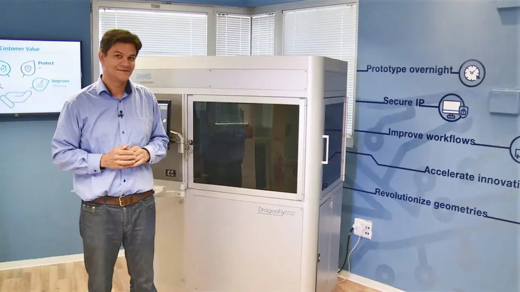
Fig.3. Mr. Simon Fried, Nano-dimension president of North America and co-founder in front of the DragonFly 2020 Pro PCB 3D printer; image credit: Nano-dimension

Selected Parameters of DragonFly 2020 Pro

  • Max PCB dimension: 20×20 cm
  • Max number of layers: up to 3mm, ~20+ layers
  • Max thickness of one board: 3mm
  • Typical layer thickness: Same as traditional PCB
  • Min dimension between conductive path: 125 μm
  • Layer Resolution: 3μm dielectric, 0.3 μm conductive silver ink
  • Inks availability: proprietary Nano-dimension only at the moment, company count with opening it for other companies in future
  • Printing cost: approx. 20-40 USD per layer of 10x10cm PCB, e.g. 200-400 USD of 10-layer 10x10cm PCB board

Summary and Conclusion

Returning back to my original question – obviously, as expected, the 3D PCB printers may not be ready soon to resolve the mass volume passive components, nevertheless it made a significant progress in past few years. In comparison to the “conventional” 3D printers – couple years ago they were considered as “prototyping tools” only and today we see some manufacturing floors full of industry grade 3D printers printing plastic or metallic structures.  Thus, in near future we may count with 3D PCB printing development as a way forward for certain application area.

are we ready to print PCBs by 3D printing?

The current capabilities of PCB 3D printing can bring already its value to mainly fast and flexible prototyping work, but also in proving of new, innovative design thoughts that would be difficult or impossible to realize by currently available technologies. In addition, you can do everything “inhouse” to protect your work without sharing it with third parties that has also its value especially for defence and military applications.

There are potential benefits also for “boring” passive components providing a new freedom to try new constructions in PCB bulk 3D space without limitations. The additional feature is capability to insert embedded components into the PCB to utilize technologies that are not possible to make by the 3D printing directly.

The 3D PCB printed is not yet dedicated to mass manufacturing (or even manufacturing) of PCBs. Nevertheless:

“The era of multi material functional printing for electronics has ushered in the ability to significantly compress the time required to develop and prototype circuits, to de-risk the development process, to allow for more freedom and experimentation, to ensure that sensitive IP stays in house for longer.” said Fried

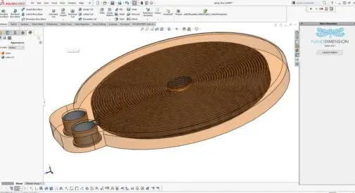
Fig.4. 3D spiral coil design in SolidWorks software ready for printing by DragonFly2020 Pro 3D printer; image credit: Nano-dimension

Further information about the DragonFly 2020 Pro and Nano-dimension company can be find at the company website https://www.nano-di.com/.

Demonstration Tech Day in the Czech Republic to see the 3D PCB printer in life will be on 18th October in Brno, Czech Republic organized by Amtech company. See the invitation and registration link here: http://news.amtech.cz/2018-08/.


Related Posts

Capacitors

Introduction of Knowles MLCCs StackiCap, its Benefits and Applications

25.5.2023
19
Capacitors

Murata Unveils Compact MLCCs with Extended Creepage Distance

25.5.2023
11
Oscillators

Properties and Characteristics of Crystal Units

24.5.2023
11

Upcoming Events

May 31
11:00 - 12:00 UTC-5

Why GFCIs with “Ground Check” Are the Future of Electrical Safety

Jun 1
June 1 @ 12:00 - June 2 @ 14:00 EDT

Space and Military Standards for Hybrids and RF Microwave Modules

Jun 13
June 13 @ 12:00 - June 16 @ 14:00 EDT

Pre Cap Visual Inspection per Mil-Std-883 (TM 2017)

View Calendar

Popular Posts

  • What is a Dielectric Constant of Plastic Materials ?

    4 shares
    Share 4 Tweet 0
  • Ripple Current and its Effects on the Performance of Capacitors

    3 shares
    Share 3 Tweet 0
  • Capacitor Selection for Coupling and Decoupling Applications

    28 shares
    Share 28 Tweet 0
  • Understanding High-Precision Resistor Temperature Coefficient of Resistance

    0 shares
    Share 0 Tweet 0
  • Leakage Current Characteristics of Capacitors

    0 shares
    Share 0 Tweet 0
  • Dielectric Constant and its Effects on the Properties of a Capacitor

    7 shares
    Share 7 Tweet 0
  • Filter Q Factor Explained

    0 shares
    Share 0 Tweet 0
  • Why Low ESR Matters in Capacitor Design

    0 shares
    Share 0 Tweet 0

Newsletter Subscription


PCNS Call for Papers !

Archive

2022
2021
2020
2019
2018
2017

Symposium

Passive Components Networking Symposium

Passives e-Learning

Knowledge Blog

  • Home
  • Privacy Policy
  • EPCI Membership & Advertisement
  • About

© EPCI - Premium Passive Components Educational and Information Site

No Result
View All Result
  • Home
  • News
  • Video
  • Knowledge Blog
  • Preferred Suppliers
  • Events

© EPCI - Premium Passive Components Educational and Information Site

Welcome Back!

Login to your account below

Forgotten Password?

Retrieve your password

Please enter your username or email address to reset your password.

Log In
This website uses cookies. By continuing to use this website you are giving consent to cookies being used. Visit our Privacy and Cookie Policy.