Passive Components Blog
No Result
View All Result
  • Home
  • NewsFilter
    • All
    • Aerospace & Defence
    • Antenna
    • Applications
    • Automotive
    • Capacitors
    • Circuit Protection Devices
    • electro-mechanical news
    • Filters
    • Fuses
    • Inductors
    • Industrial
    • Integrated Passives
    • inter-connect news
    • Market & Supply Chain
    • Market Insights
    • Medical
    • Modelling and Simulation
    • New Materials & Supply
    • New Technologies
    • Non-linear Passives
    • Oscillators
    • Passive Sensors News
    • Resistors
    • RF & Microwave
    • Telecommunication
    • Weekly Digest

    Designing a 2 kW LLC Transformer with Integrated Resonant Inductor

    Middle East Conflict: The Potential Impact to Passive Components

    Inductor Technology Dossier

    Coilcraft Releases TLVR Inductors for High Density VRMs and PoL Converters

    Rutheniums Critical Role in Passive Component Supply Chains

    Bourns Expands its Modular Contacts for Power-Dense Systems

    Murata to Decouple China Rare Earth Supply in 3 Years

    Samtec AcceleRate Slim ARC6 Cable Assemblies with New Signaling Options

    Hirose Electric to Establish Automotive Connector Plant in India

    Trending Tags

    • Ripple Current
    • RF
    • Leakage Current
    • Tantalum vs Ceramic
    • Snubber
    • Low ESR
    • Feedthrough
    • Derating
    • Dielectric Constant
    • New Products
    • Market Reports
  • VideoFilter
    • All
    • Antenna videos
    • Capacitor videos
    • Circuit Protection Video
    • Filter videos
    • Fuse videos
    • Inductor videos
    • Inter-Connect Video
    • Non-linear passives videos
    • Oscillator videos
    • Passive sensors videos
    • Resistor videos

    Thermal Modeling of Magnetics

    Standard vs Planar LLC transformers Comparison for Battery Chargers

    How Modern Tools Model Magnetic Components for Power Electronics

    Advanced Loss Modeling for Planar Magnetics in the Frenetic Planar Tool

    2026 Power Magnetics Design Trends: Flyback, DAB and Planar

    Enabling Software‑Defined Vehicle Architectures: Automotive Ethernet and Zonal Smart Power

    Calculating Resistance Value of a Flyback RC Snubber 

    One‑Pulse Characterization of Nonlinear Power Inductors

    Thermistor Linearization Challenges

    Trending Tags

    • Capacitors explained
    • Inductors explained
    • Resistors explained
    • Filters explained
    • Application Video Guidelines
    • EMC
    • New Products
    • Ripple Current
    • Simulation
    • Tantalum vs Ceramic
  • Knowledge Blog
  • DossiersNew
  • Suppliers
    • Who is Who
  • PCNS
    • PCNS 2025
    • PCNS 2023
    • PCNS 2021
    • PCNS 2019
    • PCNS 2017
  • Events
No Result
View All Result
Passive Components Blog
No Result
View All Result

Carbon Nanofibers Yield On-Chip Mini-Supercaps

24.4.2020
Reading Time: 4 mins read
A A

source: EETimes article

Julien Happich,  6/7/2016
PARIS—Founded in 2005 after having secured a number of patents leveraging the growth of carbon nanofibers (CNFs) on different substrates, Swedish startup Smoltek believes CNFs will play an essential role in shrinking IC packaging.

RelatedPosts

Designing a 2 kW LLC Transformer with Integrated Resonant Inductor

Middle East Conflict: The Potential Impact to Passive Components

Inductor Technology Dossier

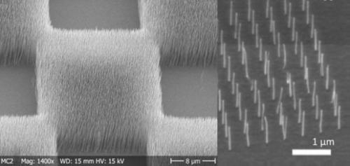
Smoltek’s core technology platform, SmolGROW is what the company claims to be the only process that enables controlled growth of conductive nanostructures at 390°C using CMOS compliant materials and processes. With this low-temperature CNF growth well under control, the company has secured an IP portfolio covering a number of applications including dense 2.5/3D stacking (SmolINPO), ultra-fine pitch interconnects (SmolINCO), integrated capacitors for energy storage or decoupling (SmolCACH), but also thermal interface materials (SmolTIM) for high performance RF and power electronics components and SmolNIL, making use of the CNFs to fabricate high aspect ratio structures through nano imprint lithography (the CNFs have a typical diameter of 50 to 100nm, being from 2 to 150 micrometres long, depending on process parameters).

Contemplating an IP licensing business model, Smoltek’s Chief Innovation Officer & Founder Dr. M. Shafiq Kabir shared his insights with EETimes Europe.

“We will licence our IP to both OSATs and foundries so they can offer the process to their customers on top of silicon, either to integrate new discrete components like our SmolCACH, or to integrate the CNFs in new packaging strategies” Kabir said in an interview.

A forest of CNFs grown onto a metal IC bond pad. (Source: Smoltek)
Click here for larger image

A forest of CNFs grown onto a metal IC bond pad. (Source: Smoltek)
“We are also working on a Process Design Kit (PDK) for the vertical integration of our process into the IC design flow, because everyone has to be aligned to optimize IC and package integration”.
The CIO revealed that his company was engaged in small projects with a number of customers, to do mostly with miniaturized interconnects exploiting the high thermal and electrical conductivity of CNFs to boost traditional micro-bumps (with copper wetting and anchored onto CNF patches).
“You could find our IP in commercial applications within the next two to three years” he said.

“With this technology, we are not aiming at replacing Through Silicon Vias (TSVs) yet, but we’ll solve the TSVs/interposer bottleneck. Copper micro-bumps don’t scale too well”, Kabir explained, “copper electro-migration impacts the lifetime reliability of silicon dies, and only CNF-based bumps will be able to scale down with future nodes”.

In a whitepaper “Using carbon nanostructures as the assembly platform in semiconductor advanced packaging beyond Moore,” the company mentions the use of selective electroplating, based on the conductive properties of CNFs to further reduce bump pitch without relying on micro solder balls. It sees a potential for 3D-shrinkage orders of magnitude (>10x-100x) compared to existing and well established bump/pillar technologies. This would allow bare dies to be stacked on each other or bonded to a substrate (interposer) or carrier (lead-frame) with much higher density interconnects.
(left) nanostructures grown in 'checker box' pattern, (right) an array of nanostructures grown on a substrate. (Source: Smoltek)Click here for larger image

(left) nanostructures grown in “checker box” pattern, (right) an array of nanostructures grown on a substrate. (Source: Smoltek)
An interesting ongoing development which could interest many OSATs doing Integrated Passive Devices (IPDs) for their customers is the SmolCACH (Capacitor on Chip) Smoltek is working on.
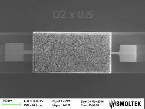
“For the moment we have achieved capacitors with moderate values in terms of capacitance per unit area for the solid state version. However the electrochemical devices show very promising results. The actual values are to be published and we’ll have to wait for some final reviews by our tech team” commented Kabir, accepting to share with us a SEM photograph of a newly manufactured ‘all solid state’ test mini supercapacitor. The SEM photograph shows a carpet of vertically grown CNFs sandwiched between two electrodes.
SEM photograph of a newly manufactured 'all solid state' test mini supercapacitor. (Source: Smoltek)Click here for larger image

SEM photograph of a newly manufactured ‘all solid state’ test mini supercapacitor. (Source: Smoltek)
“The process involves a number of lithography and materials depositions, so you may be seeing some shadows of those different layers”, commented Kabir about the faint square patterns within the rectangular shape.

“This particular device has just came out of the lab and has yet to be measured and analysed. However, we have seen an increase of a factor of 5 to 10 of the capacitance per unit area (footprint) compared to the planar counterparts in our first non-optimized version. This new batch is coming out of the lab after some optimization and we will see what it will give us” the CIO said when pressed for some characteristics.

“We are always striving to get the best values out through different technical optimizations. Some target values for performances benchmarking include over 500nF/mm2 in DC with a breakdown voltage to be superior to 2V, and over 1nF/mm2 with a breakdown voltage over 25V for RF applications”.

Last year, Smoltek’s co-founder Prof. Peter Enoksson from Chalmers University of Technology (Gothenburg, Sweden) published a paper in the Solid-State Electronics journal “CMOS compatible on-chip decoupling capacitor based on vertically aligned carbon nanofibers”, presenting on-chip decoupling capacitors of specific capacitance 55pF/µm2, 10 times higher than commercially available discrete and on-chip decoupling capacitors at the 65nm technology node, the paper claimed.

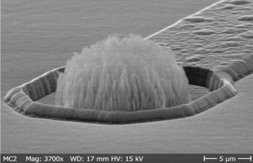
The vertically aligned CNFs were integrated directly on CMOS using a low-temperature direct current plasma enhanced chemical vapour deposition (DC-PECVD) technique. The paper explained that because the CNFs were made of cone shaped graphene layers stacked on top of each other, the nanostructures obtained had this benefit over carbon nanotubes that they consisted in a completely filled 100% metallic cylinder. Hence they achieved better conducting properties than CNTs whose typical metallic/semiconducting ratio is 1/3 when grown in bulk.

—Julien Happich is editor in chief of for EE Times Europe.
Article originally appeared on EE Times Europe.

Related

Recent Posts

Middle East Conflict: The Potential Impact to Passive Components

20.3.2026
20

Murata to Decouple China Rare Earth Supply in 3 Years

19.3.2026
102
Schematic illustration of the electric double layer of porous carbon electrodes at elevated potentials in a a conventional electrolyte and b a weakly solvating electrolyte; source: authors

Researchers Presented Lignin-based Electrolyte for 4V Supercapacitors with Low Self‑Discharge

19.3.2026
13

Samsung Outlines Growth Roadmap at its 52nd General Shareholders Meeting

19.3.2026
16

Samsung Electro-Mechanics Enters LEO Satellite Market With High‑Reliability MLCCs

19.3.2026
19

Exxelia to Exhibit at APEC 2026 in San Antonio, Texas

17.3.2026
33

ESA SPCD 26 Call for Papers Extended to 30th March

16.3.2026
83

Peak Nano to Develop Fusion Grade High Energy Film Capacitors

11.3.2026
35

Panasonic Expands Automotive PP Film Capacitors Voltage Range

9.3.2026
32

Upcoming Events

Mar 24
9:00 - 10:00 CET

Power protection in the digital age – eFuse and hot-swap strategies for modern data center design

Apr 21
16:00 - 17:00 CEST

Heatsink Solutions: Thermal Management in electronic devices

May 5
16:00 - 17:00 CEST

Understanding and Selecting Capacitors – Fundamentals, Technologies and Latest Trends

View Calendar

Popular Posts

  • Buck Converter Design and Calculation

    0 shares
    Share 0 Tweet 0
  • Boost Converter Design and Calculation

    0 shares
    Share 0 Tweet 0
  • Flyback Converter Design and Calculation

    0 shares
    Share 0 Tweet 0
  • LLC Resonant Converter Design and Calculation

    0 shares
    Share 0 Tweet 0
  • MLCC Manufacturers Consider Price Increase as AI Demand Outpaces Supply

    0 shares
    Share 0 Tweet 0
  • MLCC and Ceramic Capacitors

    0 shares
    Share 0 Tweet 0
  • Dual Active Bridge (DAB) Topology

    0 shares
    Share 0 Tweet 0
  • Ripple Current and its Effects on the Performance of Capacitors

    3 shares
    Share 3 Tweet 0
  • MLCC Case Sizes Standards Explained

    0 shares
    Share 0 Tweet 0
  • What is a Dielectric Constant and DF of Plastic Materials?

    4 shares
    Share 4 Tweet 0

Newsletter Subscription


Passive Components Blog

© EPCI - Leading Passive Components Educational and Information Site

  • Home
  • Privacy Policy
  • EPCI Membership & Advertisement
  • About

No Result
View All Result
  • Home
  • Knowledge Blog
  • PCNS

© EPCI - Leading Passive Components Educational and Information Site

This website uses cookies. By continuing to use this website you are giving consent to cookies being used. Visit our Privacy and Cookie Policy.
Go to mobile version