


This article will provide a basic discussion of connector materials and manufacturing processes.
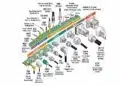
Chapter I/1.4.1 Contact Finish Electroplating on contact finishes will discuss only processes, the materials discussion will be presented in Chapter II/2.1 Contact Finishes. Chapter I/1.4.2 Copper Alloy Metallurgy and Processing will cover copper alloy metallurgy and processing from the initial casting and rolling processes to achieve the strip material that will be stamped and formed into connector contact springs. Chapter I/1.4.3 Polymer Materials and Processing will discuss polymer materials and injection molding practices for connector housings.
Contact Finish Electroplating
The majority of connector contact finishes are applied by continuous electroplating of reels of stamped and formed contacts with tin, tin-lead, silver and gold over nickel platings in thickness ranges from 0.1 to 5.0 µm (4 to 200 microinches).
Three plating practices will be described, overall, selective and duplex. In overall plating the entire contact surface is plated with a single material; tin finishes are often overall plated. In selective plating the plating is applied only to defined functional areas of the contact; gold plating is generally done selectively, with the gold applied only at the portion of the plug and receptacle contacts that define the mating interface. In duplex plating, different platings are applied at the separable connection and termination portions of the contact. The most common duplex plating is tin at the termination end, for soldering, and gold over nickel at the separable connection end. Electroplating and selective/duplex plating practices are highly proprietary and only a general description will be provided in this discussion.
Electroplating Basics
Electroplating, or electrodeposition, in connector technology refers to the plating of a material, selected for the properties discussed in Chapter I/1.2.3 Contact Finishes, onto a contact spring material, selected for the mechanical and electrical properties discussed in Chapter I/1.2.2 Contact Springs, to optimize the overall electrical performance of the plated contact system.
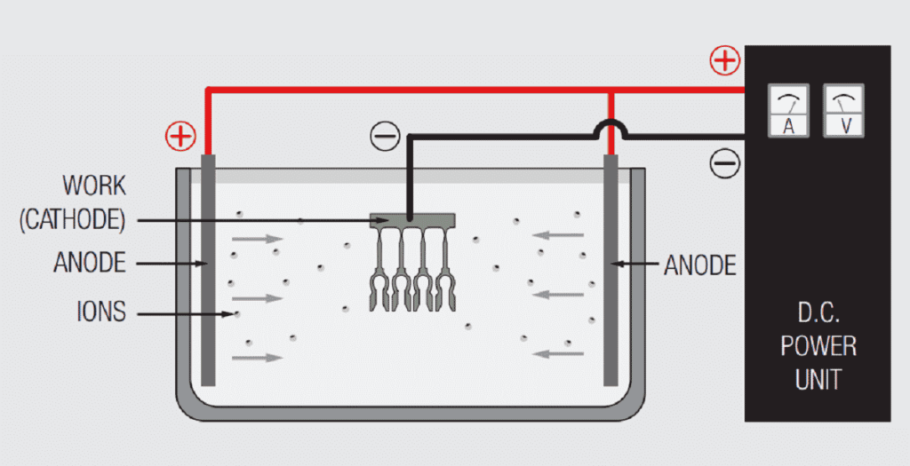
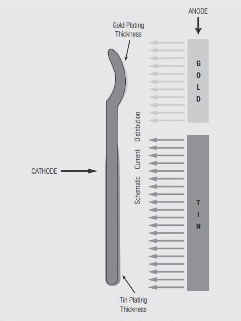
Figure 1.21 schematically illustrates a simple electrochemical plating system. The “electro” part of the system includes the voltage/current source and the electrodes, anode and cathode, immersed in the “chemical” part of the system, the electrolyte or plating bath, with the circuit being completed by the flow of ions from the plating bath to the electrodes. The metal to be deposited may be the anode and be ionized and go into solution in the electrolyte, or come from the composition of the plating bath. Copper, tin, silver and nickel metal usually comes from anodes, while gold salts are usually added to the plating bath in a controlled process to maintain the composition of the bath. The plating bath generally contains other ions to facilitate current flow between the electrodes. The deposition of metal takes place at the cathode.
The overall plating process occurs in the following sequence:
- Power supply pumps electrons into the cathode.
- An electron from the cathode transfers to a positively charged metal ion in the solution and the reduced metal plates onto the cathode.
- Ionic conduction through the plating bath completes the circuit to the anode.
- At the anode two different processes take place depending on whether the anode material is soluble, the source of the metal to be plated, or insoluble, inert. If the anode material is soluble, a metal atom gives up an electron and goes into the solution as a positively charged metal ion replenishing the metal content of the plating bath. If the anode is inert a negatively charged ion from the plating bath gives up an electron to the anode.
- The electron flows from the anode to the power supply completing the circuit.
Note that the deposition of metal at the cathode requires an electron so the rate of deposition depends on the flow of electrons, that is, the current flowing from the rectifier. The thickness of the deposit, therefore, depends on the current and the length of time the current is applied. This relationship is a result of Faraday’s law which relates the weight of a substance produced by an anodic or cathodic electrode reaction during electrolysis as being directly proportional to the quantity of electricity passed through the cell.
While Faraday’s law fixes the amount of metal deposited, the distribution of that metal is dependent on the distribution of the current. This fact allows for selective deposition of the metal, a process commonly used in connector contact electroplating. Figure 1.22 schematically illustrates the relationship between current distribution and deposited metal thickness. The same amount of current flows in the two geometries so the total metal deposited is the same, but the distribution is very different. The anode and cathode geometries and spacings in connector electroplating practice are designed to shape the current flow between the anode and cathode so as to control the deposition of the finish material, both thickness and distribution, onto the contact. This capability is critical to the successful implementation of selective and duplex plating processes. The sizes, shapes and distance between electrodes are among the proprietary processes of connector electroplating. Plating bath compositions and applied current practices may also be proprietary.
Reel-to-Reel Strip Plating
The following discussion provides a basic overview of the stages of electrodeposition during a reel-to-reel strip plating process. The manufacturing processes leading to reels of stamped and formed contacts will be described in Chapter II. The function of each stage will be described, but the details of accomplishing the function are not included because, as noted previously, electroplating practices are highly proprietary.
Stage 0 – Incoming inspection:
While inspection of the incoming reel is independent of the electroplating process, it is not overstating to say that the quality of the electroplate is controlled by the quality of the incoming reel. Successful electroplating requires a “clean” metal surface and an incoming reel with residual stamping oil, scratches or stamping damage and base metal defects may be impossible to plate so as to produce a smooth, continuous and defect free plating.
Stage 1 – Precleaning:
Given the previous comment on surface cleanliness it is not surprising that the first stage of the electroplating process is to clean the contacts. Many different cleaning processes may be included in this stage, ultrasonic organic cleaning to remove residual stamping oils or contaminants, acid, electrocleaning/electropolishing etc. A rinsing station may be included between each of the cleaning stages as well. Cleanliness is critical to electroplating success.
Stage 3 – Rinse/Dry:
On completion of electroplating the contacts are rinsed and dried before being rereeled and sent on to the next stage of the manufacturing process. Rinsing is important because residual plating solution and salts can cause corrosion of the contacts if not removed.
Multiple “Stage 2” stations can be used for multiple layer platings, gold over nickel, and, if so, it is necessary to ensure that the plating solutions do not transfer from one station to the next so a rinse station is generally included between all plating stations. In the case of gold over nickel platings, it is essential that the contacts do not dry out between the nickel and the gold stations because nickel exposed to air “passivates”, forms a thin oxide layer, inhibiting the effective plating of the following gold plate.
A few comments on selective and duplex plating are in order at this point. Figure 1.23 illustrates a contact which is both selectively and duplex plated. The first plating applied is an overall nickel underplate, that is, the entire contact surface is plated with nickel. The second plating applied is a selective gold at the mating interface, a. The third plating is a selective tin, b, at the contact tail to provide a solderable surface.
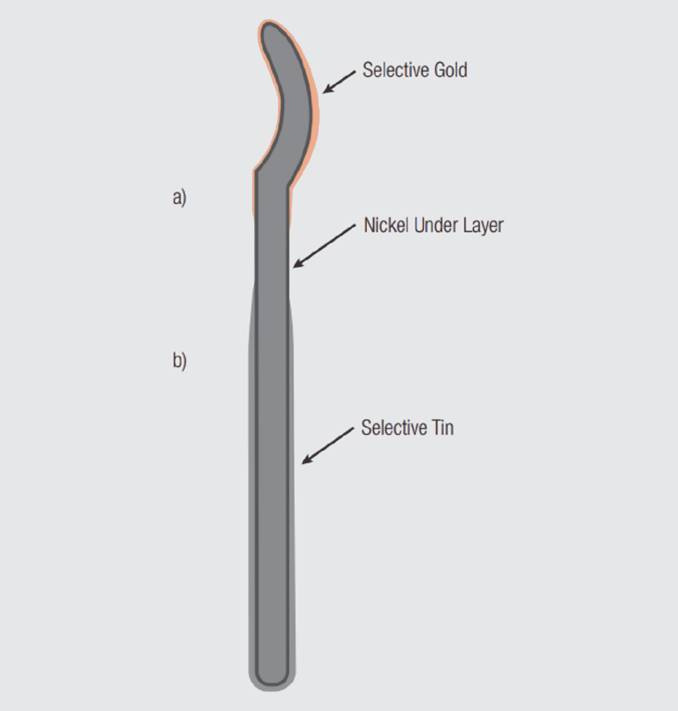
The selective plating is obvious; the tin and gold platings are applied only where needed for functionality. The contact is duplex plated because two separate areas have been plated. In this example the two platings are different, gold over nickel and tin over nickel. In some cases a gold flash is used to preserve the solderability of the contact tail section. This combination would also be considered duplex plating. If the gold flash was used, the contacts could be plated using two separate gold plating stages in the same configuration in the plating bath. The anode/cathode location and geometry would be positioned appropriately in the plating bath to plate desired areas and thicknesses. In the case of duplex tin, however, it is common to apply the gold plating and then invert the contacts in a transition stage before immersing only the contact tails into a supplementary bath to plate the tail section with tin.
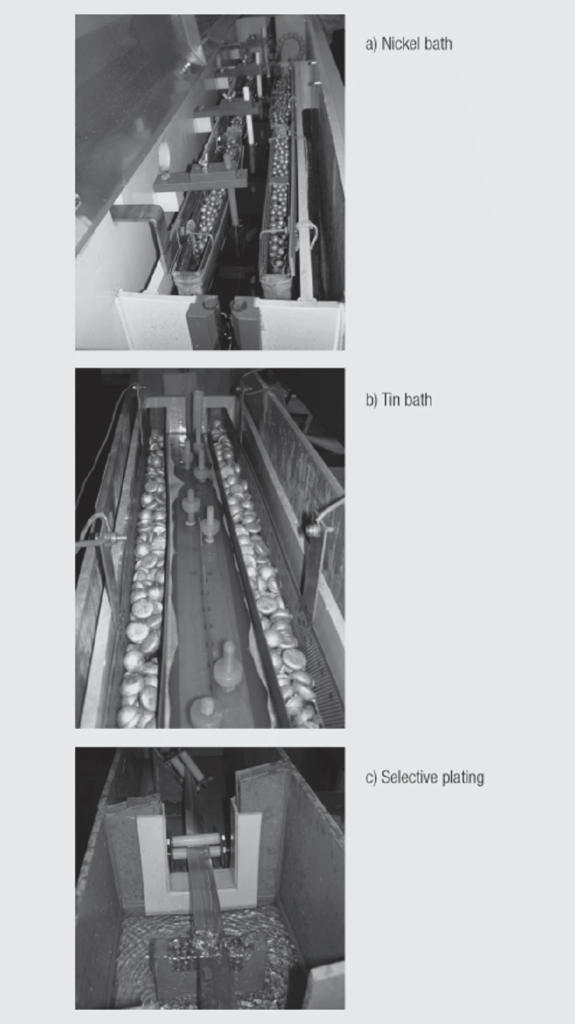
The photo of Figure 1.24 show different plating bath (a) Ni, b) Tin and c) where the bandolier pins are rotated to perform selective plating.
Contact Finish Electroplating Miscellaneous
Not all connector contacts are reel-to-reel plated. There are two batch plating processes and two non-electrolytic practices worthy of a brief discussion.
Batch Plating
The two batch plating processes differ in how the contacts are presented to the plating bath. In one case, commonly called “barrel plating” the contacts are simply placed in the barrel and incidental contact between individual contacts is relied on to retain continuity of the cathode. The contacts are generally tumbled to promote greater uniformity of plating thickness. In the second case, the contacts are attached in some manner to a frame or rack which is made the cathode during the plating process. Batch plating is used primarily for tin plated contacts intended for industrial and white goods applications.
Electroless Plating
The electrochemical reactions that give rise to electroless plating can be quite complicated. For our purposes it is sufficient to say that electroless plating consists in one metal replacing another due to a difference in electrochemical potentials without any external power, hence, electroless. Electroless plating is sometimes called immersion plating because it occurs on immersion without external power. Nickel, gold, silver and copper can be electroless plated. Benefits of electroless plating are that it plates uniformly over a surface, thus can plate into recesses and blind holes not amenable to electroplating. Limitations of electroless plating are speed and limited thickness capability, fractions of a micron. The process essentially stops when the entire surface being replaced has been covered over.
Hot Air Reflowed Tin (HART)/Hot Air Solder Leveling(HASL)
These processes are similar in that a tin or solder coating is applied and a hot air “knife” is used to level the coating. HASL is typically used in printed circuit board applications.