Passive Components Blog
No Result
View All Result
  • Home
  • NewsFilter
    • All
    • Aerospace & Defence
    • Antenna
    • Applications
    • Automotive
    • Capacitors
    • Circuit Protection Devices
    • electro-mechanical news
    • Filters
    • Fuses
    • Inductors
    • Industrial
    • Integrated Passives
    • inter-connect news
    • Market & Supply Chain
    • Market Insights
    • Medical
    • Modelling and Simulation
    • New Materials & Supply
    • New Technologies
    • Non-linear Passives
    • Oscillators
    • Passive Sensors News
    • Resistors
    • RF & Microwave
    • Telecommunication
    • Weekly Digest

    Power Converter Dossier: Passive Components Design and Selection Guide 2026

    Evans Group Unifies Four High-Rel Capacitor Leaders

    Skeleton Releases Graphene‑Based UPS for AI Data Centers

    Designing 800 V DC EMC Filters: Calculation, Simulation and Measurement

    TDK Releases DC-link Film Capacitors with Ultra-low Inductance for SiC Power Converters

    Murata Introduces World First 2.2uF 100V Soft‑Term MLCC in 0805 Size for Automotive

    Murata and Xona Partner on LEO Satellite Navigation for Industrial Applications

    Bourns Offers Custom Magnetics for 3‑Phase Flying Capacitor Inverters

    YAGEO Releases Cost Efficient Pt‑RTD Sensors with Ni wires

    Trending Tags

    • Ripple Current
    • RF
    • Leakage Current
    • Tantalum vs Ceramic
    • Snubber
    • Low ESR
    • Feedthrough
    • Derating
    • Dielectric Constant
    • New Products
    • Market Reports
  • VideoFilter
    • All
    • Antenna videos
    • Capacitor videos
    • Circuit Protection Video
    • Filter videos
    • Fuse videos
    • Inductor videos
    • Inter-Connect Video
    • Non-linear passives videos
    • Oscillator videos
    • Passive sensors videos
    • Resistor videos

    Designing 800 V DC EMC Filters: Calculation, Simulation and Measurement

    Current Sense Transformer Datasheet and Design‑in Guide

    Designing a USB Type‑C Flyback Planar Transformer with Frenetic’s Planar Tool

    Magnetics Design in High‑Frequency GaN Converters

    Qi2 Wireless Charging: Inductors, Capacitors and EMC Filters

    Two‑capacitor paradox explained for engineers

    Capacitances of Nonlinear MLCCs: What Datasheets Don’t Tell You

    Tapped Inductor Buck Converter Fundamentals

    Planar vs Conventional Transformer: When it Make Sense

    Trending Tags

    • Capacitors explained
    • Inductors explained
    • Resistors explained
    • Filters explained
    • Application Video Guidelines
    • EMC
    • New Products
    • Ripple Current
    • Simulation
    • Tantalum vs Ceramic
  • Knowledge Blog
  • DossiersNew
  • Suppliers
    • Who is Who
  • PCNS
    • PCNS 2025
    • PCNS 2023
    • PCNS 2021
    • PCNS 2019
    • PCNS 2017
  • Events
No Result
View All Result
Passive Components Blog
No Result
View All Result

Digitally Controlled Current Limiter Safely Charges Large Capacitor Banks

28.6.2018
Reading Time: 4 mins read
A A

Source: ElectronicDesign article

Ilija Uzelac | Jun 27, 2018. Using voltage feedback from the capacitor bank being charged, a MOSFET-based current-control approach applies a stepped series of increased charging currents to limit inrush current.

RelatedPosts

Power Converter Dossier: Passive Components Design and Selection Guide 2026

Evans Group Unifies Four High-Rel Capacitor Leaders

Skeleton Releases Graphene‑Based UPS for AI Data Centers

At a power-on cycle, inrush current, if not limited, can peak to tens of even hundreds of amps when capacitive load is present, thereby increasing the probability of failure and decreasing usable lifetime of a device. With large capacitor banks, an inrush current limiter is a necessary component.

A MOSFET as a voltage-controlled current device is perfectly suitable to be part of an inrush-current limiter. Power supplies with pulsed current across a current passing MOSFET at increasing duty-cycle rate are very common inrush-current limiter designs with active components. However, such designs stress the MOSFET due to currents often order of magnitude higher than the maximum safe current in a dc mode.

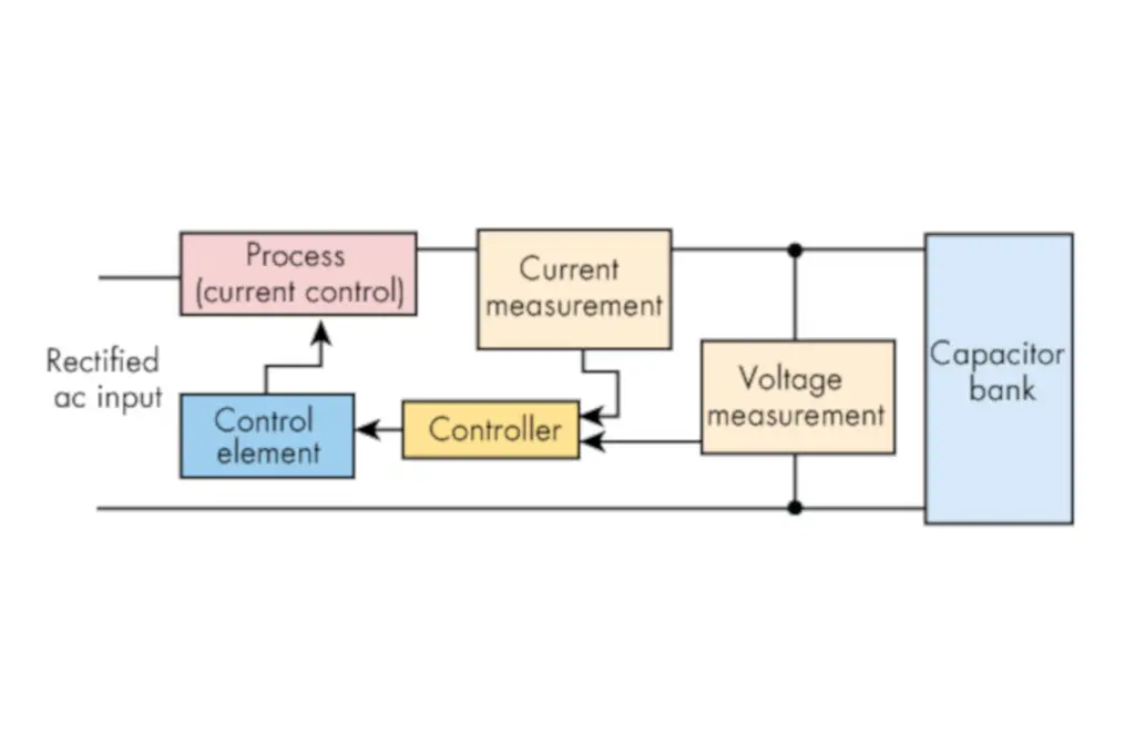
This current-limiter circuit design idea is based on a feedback-controlled current, where current across a MOSFET rises with an increase of the actual voltage across the capacitor bank Vcap(Fig. 1). Based on that voltage, a controller sets the maximum charging current while current limit is controlled through a real-time feedback sense of the charging current.

Fig 1. – see featured image. The maximum charging current is established by a controller that measures the voltage across the capacitor bank during charging cycle.

Charging current is determined based on a MOSFET safe-operating dc curve; its maximal drain current is a function of drain-to-source voltage (VDS). VDS is the difference between rectified ac input voltage, and Vcap in this design idea. Current rating also depends significantly on MOSFET temperature. For example, the datasheet for the APT75M50L N-channel MOSFET used in this design idea shows that in dc mode, the maximal current is ≈1 A at VDS = 300 V, and ≈4 A at VDS = 100 V at a case temperature of 25°C and junction temperature of 150°C.

In the practical circuit design (Fig. 2), U1 through U5 are photovoltaic MOSFET drivers. For the circuit to operate, U1’s driver is first activated via the digital on/off control pin, which in turn drives power MOSFET Q1 (the control element). With U1 active and the capacitor bank at 0 V, the charging current is set by R3, while Q2 acts as current limiter controlling the gate-source voltage of Q1. At this stage, Q3 through Q6 are not conducting and given Q2’s VBE = 0.48 V, the charging current is set and limited to 0.48 V/R3 ≈ 0.5 A. Resistors R16 through R23 form voltage dividers, providing a measure of the capacitor bank voltage for the quad comparator U6 (LM339), which uses a reference voltage of 2.5 V from the bandgap reference U7.

2. Photovoltaic gate drivers control the MOSFETs, which, in turn, control and step the current flow.

The role of each comparator is to control conductivity of branches with resistors R4 through R7 being either conductive or cut off, therefore setting different current limits depending on the Vcap. With the given resistor values, comparators U6A to U6D will be triggered when the Vcap exceeds approximately 60 V, 120 V, 175 V and 215 V, and will make branches with R4 through R7 respectively conductive.

For example, when the Vcap exceeds 60 V, it will trigger comparator U6A, setting its output low. This turns on MOSFET driver U2, driving Q3 into a fully conductive mode, and the branch with R4 will start to conduct current in parallel with R3. The charging current passing through Q1 is now determined by a parallel combination of resistors R3 and R4 + RDS (the on-resistance of Q3, maximum value 40 mΩ), while Q2 maintains the same current-limiting function. The new current limit is 0.48 V/(R3 || (R4 + RDS) ≈ 0.9 A.

A printed-circuit board was built and tested extensively to prove the robustness and efficiency of this circuit. The input voltage is rectified 240 V ac from a 120/240-V ac transformer. The charging current was measured across a 1-Ω resistor with an isolated oscilloscope probe. The approximate maximum current levels were 0.5 A for Vcap of 0 to 60 V; 0.9 A for Vcap of 60 to 120 V; 1.5 A for Vcap of 120 to 180 V; 2.25 A for Vcap of 180 to 215 V; and 5.7 A for Vcap above 215 V.

3. The voltage versus time graph shows inflection points (knees) where the charging current changes.

In the graph of the Vcap during its charging cycle (Fig. 3), the different knee points illustrate different charging currents, quantified with a changing slope of the line. Resistors R1 and R8 through R11 are fail-safe measures that keep the MOSFETs shut off in a case of open-circuit failure of photovoltaic MOSFET drivers. VCC can be either 3.3 V or 5 V with the given resistor values, or higher if resistor values R2, R12 to R15, and R24 are appropriately re-scaled.

Ilija Uzelac is a Research Scientist at Georgia Institute of Technology, with a PhD in Physics from Vanderbilt University, and a Master’s in Electrical Engineering from University of Belgrade, Serbia.

References

1) Ilija Uzelac, “Feedback-Controlled Constant-Current Limiter Includes Digital On/Off Control,” Electronic Design.

2) Ilija Uzelac and Ron Reiserer, “Series-connected MOSFETs increase voltage & power handling,” EDN.

Related

Recent Posts

Power Converter Dossier: Passive Components Design and Selection Guide 2026

5.6.2026
8

Evans Group Unifies Four High-Rel Capacitor Leaders

5.6.2026
11

Skeleton Releases Graphene‑Based UPS for AI Data Centers

5.6.2026
10

Designing 800 V DC EMC Filters: Calculation, Simulation and Measurement

4.6.2026
50

TDK Releases DC-link Film Capacitors with Ultra-low Inductance for SiC Power Converters

4.6.2026
33

Murata Introduces World First 2.2uF 100V Soft‑Term MLCC in 0805 Size for Automotive

4.6.2026
18

Nvidia Vera Rubin: Why One AI Rack Needs So Many More MLCC Capacitors

2.6.2026
150

Tecate Unveils High‑temp 105C Supercapacitors for Harsh‑Environment Designs

2.6.2026
17

Passive Components in 2026: From Invisible Commodity to Design Parameter

2.6.2026
57

Upcoming Events

Jun 16
16:00 - 17:00 CEST

EMC with EMC – EMC‑compliant design with electromechanical connectors

View Calendar

Popular Posts

  • Buck Converter Design and Calculation

    0 shares
    Share 0 Tweet 0
  • Boost Converter Design and Calculation

    0 shares
    Share 0 Tweet 0
  • MLCC and Ceramic Capacitors

    0 shares
    Share 0 Tweet 0
  • Flyback Converter Design and Calculation

    0 shares
    Share 0 Tweet 0
  • LLC Resonant Converter Design and Calculation

    0 shares
    Share 0 Tweet 0
  • Dual Active Bridge (DAB) Topology

    0 shares
    Share 0 Tweet 0
  • What Electronics Engineer Needs to Know About Passive Low Pass Filters

    0 shares
    Share 0 Tweet 0
  • Capacitor Charging and Discharging

    0 shares
    Share 0 Tweet 0
  • SEPIC Converter Design and Calculation

    0 shares
    Share 0 Tweet 0
  • Earthing Systems and IEC Classification Explained

    0 shares
    Share 0 Tweet 0

Newsletter Subscription


Passive Components Blog

© EPCI - Leading Passive Components Educational and Information Site

  • Home
  • Privacy Policy
  • EPCI Membership & Advertisement
  • About

No Result
View All Result
  • Home
  • Knowledge Blog
  • Dossiers
  • PCNS

© EPCI - Leading Passive Components Educational and Information Site

This website uses cookies. By continuing to use this website you are giving consent to cookies being used. Visit our Privacy and Cookie Policy.
Go to mobile version