





Passive Components Blog
No Result
View All Result
  • Home
  • News
    • All
    • Aerospace & Defence
    • Antenna
    • Applications
    • Automotive
    • Capacitors
    • Circuit Protection Devices
    • electro-mechanical news
    • Filters
    • Fuses
    • Inductors
    • Industrial
    • Integrated Passives
    • inter-connect news
    • Market & Supply Chain
    • Market Insights
    • Medical
    • Modelling and Simulation
    • New Materials & Supply
    • New Technologies
    • Non-linear Passives
    • Optoelectronics and Isolation
    • Oscillators
    • Passive Sensors News
    • Resistors
    • RF & Microwave
    • Telecommunication
    • Weekly Digest
    Vishay Sfernice D2TO and DTO thick-film SMD power resistor sample kits with TO-263 D2PAK and TO-252 DPAK devices

    Vishay SMD Power Resistor Sample Kits for High-Power Design

    schurter-tcsv4-side-actuated-smt-tactile-switch

    SCHURTER Introduces Side-Actuated SMT Tactile Switch

    TLVR multiphase coupled inductors, auxiliary ballast inductor

    TLVR Coupled Inductors: Fast Load-Step Response and Current-Dependent Ballast-Inductor Optimisation

    Bourns CRH2512 2512 surface-mount metal-alloy current-sense resistor for high-current low-ohmic measurement

    Bourns CRH2512 5 W Current-Sense Resistors

    Littelfuse AK-FL FlatSuppressX axial-leaded bidirectional TVS diodes for high-voltage aviation DC power protection

    Littelfuse AK-FL TVS Diodes for Aviation DC Power Rails

    Rheinmetall Pierburg Pump Technology NanoLam DC-link capacitors for high-power electric vehicle traction inverter applications

    Rheinmetall Funds NanoLam Capacitor Production Scale-Up

    Bourns CSS4C-1216 four-terminal metal-strip current sense resistor for high-current Kelvin measurement

    Bourns Extends 1216 Kelvin Current Sense Resistors

    Modelithics COMPLETE+3D Library v26.3 for Ansys HFSS with RF passive component and 3D electromagnetic simulation models

    Modelithics COMPLETE+3D v26.3 Expands HFSS RF Models

    Samsung Electro-Mechanics low-profile and embedded MLCCs for compact PCB and power-delivery applications

    Samsung Low-Profile and Embedded MLCCs for Compact Devices

    Trending Tags

    • Ripple Current
    • RF
    • Leakage Current
    • Tantalum vs Ceramic
    • Snubber
    • Low ESR
    • Feedthrough
    • Derating
    • Dielectric Constant
    • New Products
    • Market Reports
  • Knowledge Blog
  • Dossiers
    • AI Hardware Dossier
    • Automotive Dossier
    • Industrial Robotics Dossier
    • Power Converter Dossier
    • Capacitor Dossier
    • Resistor Dossier
    • Inductor Dossier
    • Circuit Protection Dossier
  • Suppliers
    • Who is Who
  • PCNS
    • PCNS 2025
    • PCNS 2023
    • PCNS 2021
    • PCNS 2019
    • PCNS 2017
  • Events
  • Home
  • News
    • All
    • Aerospace & Defence
    • Antenna
    • Applications
    • Automotive
    • Capacitors
    • Circuit Protection Devices
    • electro-mechanical news
    • Filters
    • Fuses
    • Inductors
    • Industrial
    • Integrated Passives
    • inter-connect news
    • Market & Supply Chain
    • Market Insights
    • Medical
    • Modelling and Simulation
    • New Materials & Supply
    • New Technologies
    • Non-linear Passives
    • Optoelectronics and Isolation
    • Oscillators
    • Passive Sensors News
    • Resistors
    • RF & Microwave
    • Telecommunication
    • Weekly Digest
    Vishay Sfernice D2TO and DTO thick-film SMD power resistor sample kits with TO-263 D2PAK and TO-252 DPAK devices

    Vishay SMD Power Resistor Sample Kits for High-Power Design

    schurter-tcsv4-side-actuated-smt-tactile-switch

    SCHURTER Introduces Side-Actuated SMT Tactile Switch

    TLVR multiphase coupled inductors, auxiliary ballast inductor

    TLVR Coupled Inductors: Fast Load-Step Response and Current-Dependent Ballast-Inductor Optimisation

    Bourns CRH2512 2512 surface-mount metal-alloy current-sense resistor for high-current low-ohmic measurement

    Bourns CRH2512 5 W Current-Sense Resistors

    Littelfuse AK-FL FlatSuppressX axial-leaded bidirectional TVS diodes for high-voltage aviation DC power protection

    Littelfuse AK-FL TVS Diodes for Aviation DC Power Rails

    Rheinmetall Pierburg Pump Technology NanoLam DC-link capacitors for high-power electric vehicle traction inverter applications

    Rheinmetall Funds NanoLam Capacitor Production Scale-Up

    Bourns CSS4C-1216 four-terminal metal-strip current sense resistor for high-current Kelvin measurement

    Bourns Extends 1216 Kelvin Current Sense Resistors

    Modelithics COMPLETE+3D Library v26.3 for Ansys HFSS with RF passive component and 3D electromagnetic simulation models

    Modelithics COMPLETE+3D v26.3 Expands HFSS RF Models

    Samsung Electro-Mechanics low-profile and embedded MLCCs for compact PCB and power-delivery applications

    Samsung Low-Profile and Embedded MLCCs for Compact Devices

    Trending Tags

    • Ripple Current
    • RF
    • Leakage Current
    • Tantalum vs Ceramic
    • Snubber
    • Low ESR
    • Feedthrough
    • Derating
    • Dielectric Constant
    • New Products
    • Market Reports
  • Knowledge Blog
  • Dossiers
    • AI Hardware Dossier
    • Automotive Dossier
    • Industrial Robotics Dossier
    • Power Converter Dossier
    • Capacitor Dossier
    • Resistor Dossier
    • Inductor Dossier
    • Circuit Protection Dossier
  • Suppliers
    • Who is Who
  • PCNS
    • PCNS 2025
    • PCNS 2023
    • PCNS 2021
    • PCNS 2019
    • PCNS 2017
  • Events
No Result
View All Result
Passive Components Blog
No Result
View All Result

How to design a high voltage DCM inverting charge pump converter

7.2.2019
Reading Time: 4 mins read
A A

Source: EDN article

Power Tips #87: How to design a high voltage DCM inverting charge pump converter. By John Betten

RelatedPosts

Vishay SMD Power Resistor Sample Kits for High-Power Design

SCHURTER Introduces Side-Actuated SMT Tactile Switch

TLVR Coupled Inductors: Fast Load-Step Response and Current-Dependent Ballast-Inductor Optimisation

A low-current, negative high-voltage is required to bias sensors in advanced driver assistance systems, ultrasonic transducers for sonar applications and communications equipment. Flyback, Cuk and inverting buck-boost converters are all possible solutions, but are penalized by bulky transformers (flyback and Cuk) or limited in their maximum negative voltage by the controller’s input-voltage rating (inverting buck-boost). In this power tip, I’ll detail the operation of a converter that pairs a single inductor with an inverting charge pump operating in discontinuous conduction mode (DCM).  Paired with a ground referenced boost controller, a large negative output voltage can be generated at a lower system cost.

Figure 1 shows a simplified power-stage schematic. Note that this schematic is different from a traditional inverting buck-boost converter, which “floats” the controller between VIN and -VOUT. In that converter, the maximum -VOUT achievable is the maximum VCC of the controller minus the maximum input voltage. This would make it nearly impossible to find a controller that can drive an N-channel field-effect transistor (FET) for an output voltage of -100 V or more.

Figure 1 Simplified power stage of an inductor-driven inverting charge pump.

The circuit’s operation can be split into three intervals, detailed in Figure 2. In the first interval, the FET is on during duty cycle (d), which applies VIN across the inductor, allowing current to ramp up from zero, storing energy. However, in the previous cycle, C1 (which maintains a voltage of approximately equal to VOUT) has depleted its excess stored energy, reverse-biasing D1 and D2. This is why D1, D2 and C1 are not shown in this interval. C2 supplies all load current.

In the next interval, d’, the FET turns off and the inductor current begins to discharge, causing its voltage polarity to reverse. This greatly increases the voltage present at node VFET, allowing C1 to recharge through D1. During this interval, current ramps downward until D1 turns off. However, due to the reverse-recovery characteristics of D1, current goes negative before it eventually turns off, at which point the inductor current slope changes and its voltage polarity reverses once again.

The third interval, d’’, is when the energy transfer from C1 to C2 takes place. When D1 stops conducting, the inductor voltage is clamped to VIN because the VFET node voltage is forced to ground by a current path through the FET’s body diode. Current flows through D2 until the voltages across C1 and C2 equalize, but current through the FET’s body diode continues until the inductor’s current reaches zero. At this point, the voltage across the inductor collapses and resonates with circuit parasitics until the FET turns on again.


Figure 2 The three phases of DCM operation.

Figure 3 details the key voltage and current waveforms. DCM operation allows for the smallest possible inductance, but with a higher peak current. Inductance for DCM operation is determined at the maximum duty cycle, minimum VIN and full load. Carefully check the maximum duty cycle against the controller data sheet, but you can typically choose 60%-90%, or otherwise pulse skipping can occur. Larger inductances will push operation into continuous conduction mode (CCM), since the current will not return to zero before the next switching cycle. This results in using an inductor that may be larger than necessary and requires extra care to prevent subharmonic oscillation.

Figure 3 Key circuit waveforms in DCM.

Design equations

For DCM operation, Equation 1 satisfies the relationship involving the inductor’s stored energy:

where ipk is the peak inductor current and η is the converter’s efficiency. The peak inductor current is then equal to Equation 2:

From the following two equations, Equation 3 expresses the duty cycle (d) in terms of :

Since VIN is the voltage across the inductor when the FET is on and ipk is the inductor current at the end of duty cycle d, substituting Equation 2 into Equation 3 yields Equations 4 and 5:

The average load current is determined by the geometric relationship in Equations 6 and 7 during interval d’:

Substituting Equation 2 into Equation 7 provides Equation 8:


The remainder of the period is defined as d’’, which is when the energy transfers into C2 and the remaining inductor current discharges to zero (Equation 9):

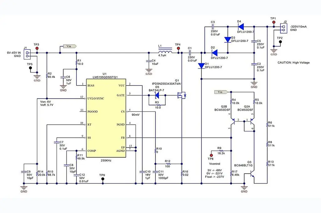
Figure 4 shows an example schematic implementing this converter with a voltage doubler, which allows the voltage stress of each power-stage component to be equal to one-half of the full output voltage. This provides a wider selection of components from which to choose. In this application, the inductance was calculated as if the output voltage was one-half, but at twice the load current.

featured image and Figure 4 Inductor-driven inverting charge pump with voltage doubler and level-shifting current mirror schematic

This converter provides a small, single-inductor solution for generating a large negative voltage. Additionally, it allows the use of an inexpensive ground-referenced boost controller to drive an N-channel FET.

For more Power Tips, check out TI’s Power Tips blog series on Power House.

Related

Recent Posts

TLVR multiphase coupled inductors, auxiliary ballast inductor

TLVR Coupled Inductors: Fast Load-Step Response and Current-Dependent Ballast-Inductor Optimisation

24.9.2026
18

Bourns Adds ACXX57SQ Air Coil Inductors for RF Design

18.9.2026
16
Frenetic planar ER transformer simulation for a 5 kW 800 V-to-50 V PSFB converter, showing low-profile core geometry and high-current planar winding arrangement

5 kW 800 V-to-50 V PSFB Transformer Design for Data Centers

18.9.2026
45

On-Chip 3D-Printed Copper Microinductors: A New Route to Compact RF Electronics

10.9.2026
36
Murata DLW32SH_MF 1210 surface-mount common mode choke coil with metal terminals for automotive CAN FD signal-line noise suppression

Murata Introduces Common Mode Chokes for Automotive CAN FD up to 150°C

10.9.2026
46
onsemi solid-state transformer concept for 800 V HVDC AI data center power conversion with SiC modules, DC-link capacitors and high-frequency magnetics

Solid-State Transformers for 800 V AI Data Centers: Passive Component Design Considerations

9.9.2026
156

Coilcraft Introduces Automotive Common Mode Chokes Target CISPR 25 Class 5 EMC Compliance

7.9.2026
32

Murata Expands Automotive Metal Power Inductor Range

7.9.2026
49

August 2026 Interconnect, Passives and Electromechanical Components Market Insights

4.9.2026
66

Upcoming Events

Sep 29
16:00 - 17:00 CEST

Cybersecurity 2026

Sep 30
15:00 - 16:00 CEST

Positronic Space and Military Connectors

Oct 14
17:00 - 18:00 CEST

Live Demo! Discover KYOCERA AVX Antenna Integrator Studio (AIS)

View Calendar

Popular Posts

  • Buck Converter Design and Calculation

    0 shares
    Share 0 Tweet 0
  • LLC Resonant Converter Design and Calculation

    0 shares
    Share 0 Tweet 0
  • Boost Converter Design and Calculation

    0 shares
    Share 0 Tweet 0
  • Flyback Converter Design and Calculation

    0 shares
    Share 0 Tweet 0
  • Capacitor Charging and Discharging

    0 shares
    Share 0 Tweet 0
  • Resistor Symbols

    0 shares
    Share 0 Tweet 0
  • Thermistors Basics, NTC and PTC Thermistors

    0 shares
    Share 0 Tweet 0
  • Audio Capacitors: Choosing Capacitors for Crossover Circuits

    0 shares
    Share 0 Tweet 0
  • Capacitor Symbols

    0 shares
    Share 0 Tweet 0
  • MLCC and Ceramic Capacitors

    0 shares
    Share 0 Tweet 0

Newsletter Subscription


Passive Components Blog

© 2015–2026
All rights reserved

  • Home
  • Privacy Policy
  • EPCI Membership & Advertisement
  • About

No Result
View All Result
  • Home
  • Knowledge Blog
  • Dossiers
  • PCNS

© 2015–2026
All rights reserved