Passive Components Blog
No Result
View All Result
  • Home
  • NewsFilter
    • All
    • Aerospace & Defence
    • Antenna
    • Applications
    • Automotive
    • Capacitors
    • Circuit Protection Devices
    • electro-mechanical news
    • Filters
    • Fuses
    • Inductors
    • Industrial
    • Integrated Passives
    • inter-connect news
    • Market & Supply Chain
    • Market Insights
    • Medical
    • Modelling and Simulation
    • New Materials & Supply
    • New Technologies
    • Non-linear Passives
    • Oscillators
    • Passive Sensors News
    • Resistors
    • RF & Microwave
    • Telecommunication
    • Weekly Digest

    Vishay Releases Miniature SMD Trimmers for Harsh Environments

    Würth Elektronik Releases Push-Button and Main Switches

    Littelfuse Unveils High-Precision TMR Angle Magnetic Sensors

    Stackpole Extends Voltage of High Temp Chip Resistors

    High Voltage MLCCs Meeting the Growing Demand for Efficiency in Power Conversion

    Bourns Releases High Power High Ripple Chokes

    KYOCERA AVX Releases Hermaphroditic WTW and WTB Connectors

    Radiation Tolerance of Tantalum and Ceramic Capacitors

    TDK Releases Compact Polypropylene Film Capacitors for Resonant Topologies

    Trending Tags

    • Ripple Current
    • RF
    • Leakage Current
    • Tantalum vs Ceramic
    • Snubber
    • Low ESR
    • Feedthrough
    • Derating
    • Dielectric Constant
    • New Products
    • Market Reports
  • VideoFilter
    • All
    • Antenna videos
    • Capacitor videos
    • Circuit Protection Video
    • Filter videos
    • Fuse videos
    • Inductor videos
    • Inter-Connect Video
    • Non-linear passives videos
    • Oscillator videos
    • Passive sensors videos
    • Resistor videos

    Percolation Phenomenon and Reliability of Molded Power Inductors in DC/DC converters

    Root Causes and Effects of DC Bias and AC in Ceramic Capacitors

    How to Calculate the Output Capacitor for a Switching Power Supply

    Switched Capacitor Converter Explained

    Understanding Inductor Dot Markings and Their Application in LTspice

    Accelerating Full Bridge LLC Resonant Converter Design with Frenetic AI

    Understanding Switched Capacitor Converters

    Coupled Inductors Circuit Model and Examples of its Applications

    Inductor Resonances and its Impact to EMI

    Trending Tags

    • Capacitors explained
    • Inductors explained
    • Resistors explained
    • Filters explained
    • Application Video Guidelines
    • EMC
    • New Products
    • Ripple Current
    • Simulation
    • Tantalum vs Ceramic
  • Knowledge Blog
  • Suppliers
    • Who is Who
  • Events
No Result
View All Result
Passive Components Blog
No Result
View All Result

Reducing conducting thin film surface roughness for electronics

9.3.2017
Reading Time: 3 mins read
A A

source: Science Daily news

As transistor dimensions within integrated circuits continue to shrink, smooth metallic lines are required to interconnect these devices. If the surfaces of these tiny metal lines aren’t smooth enough, it substantially reduces their ability to conduct electrical and thermal energy — decreasing functionality. Engineers report an advance in modeling results that establish electrical surface treatment of conducting thin films as a physical processing method for reducing surface roughness.

RelatedPosts

Vishay Releases Miniature SMD Trimmers for Harsh Environments

Würth Elektronik Releases Push-Button and Main Switches

Littelfuse Unveils High-Precision TMR Angle Magnetic Sensors

A group of engineers at the University of Massachusetts Amherst are now reporting an advance this week in Applied Physics Letters, from AIP Publishing, in the form of modeling results that establish electrical surface treatment of conducting thin films as a physical processing method for reducing surface roughness.

“We’ve been thinking hard about this roughness problem for many years, since showing that electric currents can be used to inhibit surface cracking,” said Dimitrios Maroudas, co-author and a professor in the Department of Chemical Engineering. “So as soon as we developed the computational tools to attack the full film roughness problem, we got to work.”

The group’s work focused on using a copper film on a silicon nitride layer to quantify the model parameters for their simulations and make comparisons with available experimental findings, which they were able to reproduce.

“Surface electromigration is the key physical concept involved,” Maroudas explained. “It’s the directed transport of atoms on the metal surface due to the so-called electron wind force, which expresses the transfer of momentum from the electrons of the metal moving under the action of an electric field to the atoms (ions) — biasing atomic migration.”

Think of it as akin to the diffusion of ink in flowing water. “Electromigration’s role in the transport of surface atoms is analogous to that of convection due to flow on the transport of ink within the water,” Maroudas said. “The combined effects of a well-controlled applied electric field and rough surface geometry drive the atoms on the metal surface to move from the hills of the rough surface morphology to the neighboring valleys, which eventually smooth away the rough surfaces.”

This work is significant, particularly within the microelectronics realm, because it establishes the electrical treatment of metallic (conducting) films as a viable physical processing strategy for reducing their surface roughness.

“Our approach is qualitatively different than traditional mechanical polishing or ion-beam irradiation techniques,” said Lin Du, co-author and a doctoral student working with Maroudas. “It directly influences the driven diffusion of surface atoms precisely, which affects surface atomic motion and enables a smooth surface all the way down to the atomic level.”

The required electric field action can be conveniently controlled macroscopically: simply choose a direction, adjust the voltage, and flip a switch “on.”

“While studying the phenomenon, we discovered that a sufficiently strong electric field can bring the metallic surface to an atomically smooth state,” Du said. “The required electric field strength depends largely on the field direction and surface material properties of the metallic film — such as film texture and surface diffusional anisotropy, because in surfaces of crystalline materials diffusion is faster along certain preferred directions.”

A true irony here is that “electromigration is best known for its damaging effects within metallic interconnects — underlying crucial materials reliability problems in many generations of microelectronics,” Maroudas said.

As far as applications, since this work establishes the principles to create smoother conducting material surfaces, “it can be used for fabricating and processing nanoscale-thick metallic components within electronic and optical devices, which require atomic-scale smoothness,” Maroudas said. “The ability to reduce the surface roughness of metallic components, such as interconnects within integrated circuits, will significantly improve their performance as well as durability and reliability.”

What’s the next step for the engineers? “We’re currently exploring how the effectiveness of the method depends on the metallic film texture (or surface crystallographic orientation), the film’s wetting of the substrate, and the electric field direction with respect to certain surface crystallographic directions,” Maroudas said.

The group’s immediate goal is “to optimize the electrical treatment technique, and to identify the conditions for minimizing the required electric field strength, as well as the cost of applying this technique,” he added. “Our next natural step should be a partnership with an experimental laboratory with the proper expertise to carry out tests that will help us move from proof of concept to an enabling technology.”

Story Source: Materials provided by American Institute of Physics. Note: Content may be edited for style and length.

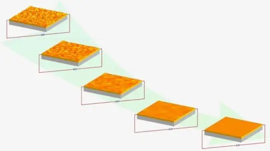
Featured Image: Sequence of snapshots from a computer simulation of electric-field-driven morphological evolution of a copper thin film, demonstrating current-induced smooth surface. Credit: Du and Maroudas

Related

Recent Posts

Vishay Releases Miniature SMD Trimmers for Harsh Environments

14.8.2025
3

Littelfuse Unveils High-Precision TMR Angle Magnetic Sensors

13.8.2025
4

Stackpole Extends Voltage of High Temp Chip Resistors

13.8.2025
6

High Voltage MLCCs Meeting the Growing Demand for Efficiency in Power Conversion

12.8.2025
44

Bourns Releases High Power High Ripple Chokes

8.8.2025
25

Radiation Tolerance of Tantalum and Ceramic Capacitors

8.8.2025
60

TDK Releases Compact Polypropylene Film Capacitors for Resonant Topologies

7.8.2025
31

Percolation Phenomenon and Reliability of Molded Power Inductors in DC/DC converters

6.8.2025
34

Root Causes and Effects of DC Bias and AC in Ceramic Capacitors

6.8.2025
47

Knowles Unveils High-Performance Safety-Certified MLCC Capacitors

6.8.2025
39

Upcoming Events

Sep 22
September 22 @ 13:00 - September 25 @ 15:15 EDT

Pre Cap Visual Inspection per Mil-Std-883 (TM 2017)

Sep 30
September 30 @ 12:00 - October 2 @ 14:00 EDT

MIL-Std-883 TM 2010

Oct 17
12:00 - 14:00 EDT

External Visual Inspection per MIL-STD-883 TM 2009

Oct 21
October 21 @ 12:00 - October 23 @ 14:15 EDT

Space and Military Standards for Hybrids and RF Microwave Modules

Nov 4
November 4 @ 12:00 - November 6 @ 14:15 EST

Wirebond Materials, Processes, Reliability and Testing

View Calendar

Popular Posts

  • Buck Converter Design and Calculation

    0 shares
    Share 0 Tweet 0
  • Boost Converter Design and Calculation

    0 shares
    Share 0 Tweet 0
  • Flyback Converter Design and Calculation

    0 shares
    Share 0 Tweet 0
  • LLC Resonant Converter Design and Calculation

    0 shares
    Share 0 Tweet 0
  • What is a Dielectric Constant and DF of Plastic Materials?

    4 shares
    Share 4 Tweet 0
  • Ripple Current and its Effects on the Performance of Capacitors

    3 shares
    Share 3 Tweet 0
  • Dual Active Bridge (DAB) Topology Explained

    0 shares
    Share 0 Tweet 0
  • How to Design an Inductor

    0 shares
    Share 0 Tweet 0
  • MLCC Case Sizes Standards Explained

    0 shares
    Share 0 Tweet 0
  • MLCC and Ceramic Capacitors

    0 shares
    Share 0 Tweet 0

Newsletter Subscription


Passive Components Blog

© EPCI - Leading Passive Components Educational and Information Site

  • Home
  • Privacy Policy
  • EPCI Membership & Advertisement
  • About

No Result
View All Result
  • Home
  • Knowledge Blog
  • Premium Suppliers

© EPCI - Leading Passive Components Educational and Information Site

This website uses cookies. By continuing to use this website you are giving consent to cookies being used. Visit our Privacy and Cookie Policy.
Go to mobile version