This paper presents development of SMD compatible Ku-band Low-temperature co-fired ceramic (LTCC) circulators. N. Parker Université de Bretagne at col. from IMT Atlantique and Thales (France), presented this during the 5th Space Passive Component Days (SPCD), an International Symposium held from October 15th to 18th, 2024, at ESA/ESTEC in Noordwijk, the Netherlands. Published under permission from ESA SPCD organizers.
LTCC technology is explored for designing compact and cost-effective surface-mountable device (SMD) circulators. The design process involves optimizing the SMD transition topology, considering the LTCC manufacturing constraints, and simulating the performance of the Y-junction circulator with a circular resonator. The simulations demonstrate good performance with low losses in the Ku-band frequency range.
Low-loss circulators using LTCC technology compatible with SMD technology have been successfully produced and soldered to a printed circuit board. The performance of the soldered circulators was measured, showing good agreement with simulated results, with a wider bandwidth observed for the spinel ferrite circulator. This work represents a significant advancement in the field of microwave circulator technology.
The high cost, large size, and complex integration of Y-junction circulators are addressed by the low-temperature co-fired ceramic (LTCC) technology. LTCC streamlines the production process, yielding a monolithic substrate that decreases fabrication costs.
Good performance with low losses can be achieved in Ku-band using LTCC. This paper aims to mitigate compactness and ease of integration, which are the other two main downsides. The 2.5D nature of LTCC allows the integration of solder pads and vias compatible with surface-mounted component (SMD) technology into the substrate.
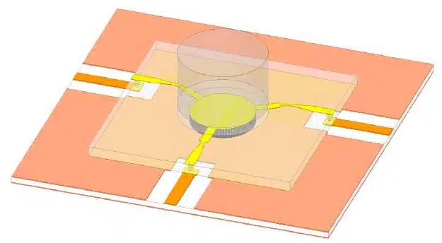
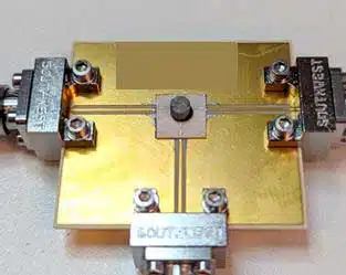
The circulator and PCB structure are shown in Fig. 1. The metallization topology is a Y-junction in microstrip topology, made of silver. A permanent magnet on a dielectric spacer polarizes the ferrite.
The design of SMD circulators compatible with LTCC will be described. Fabrication steps and measurements of two circulators based on garnet or spinel ferrites will be detailed.
Material Properties And Simulation Configuration
The permanent magnet, a Samarium-Cobalt Magsy magnet (reference YXG-28), is placed on a 300µm Teflon spacer due to its high conductivity. The substrate of the circulator consists of a high permittivity dielectric, which houses the SMD connectors and access lines, and a ferrite disc positioned under the central circular resonator. The ferrites used are a garnet ferrite and a spinel ferrite whose sintering temperature is below 950°C. They have been specifically developed to be compatible with the LTCC technology and to be used in circulators. They have previously been used in [6]. The garnet ferrite exhibits moderate saturation magnetization but high permittivity, while the spinel ferrite exhibits high magnetization and moderate permittivity.
The simulation software used is the Ansys HFSS electromagnetic solver. The internal magnetic field inside the ferrite, generated by the permanent magnet, is determined by the Ansys Maxwell3D magnetostatic solver. Doing so allows the non-uniformity of the static field inside the ferrite to be accounted for.
The SMD transitions and Y-junction are designed separately and then combined to simulate the SMD component.
| Material | εr | tanδ | 4πMs (G) | ΔH (Oe) |
| Garnet | 21 | 3.10-3 | 1900 | 100 |
| Spinel | 13 | 1.10-3 | 3800 | 100 |
| VLF220Aq4 | 21 | 1.10-3 | – | – |
| Teflon™ | 2.1 | 1.10-3 | – | – |
The SMD transition uses a metallized half-via at the substrate edge. However, LTCC manufacturing requires a modified transition, especially regarding the via.
The component thickness is 352µm, with four material layers. The two faces are connected by a 100µm via. Each layer must be metallized independently before assembly. The vias are metallized using a circular 200µm diameter pattern, resulting in metallized circles at the layer interfaces. The PCB substrate is a 203µm Rogers 4003 sheet.
Simulation of a soldered microstrip line shows a return loss over 20dB in the frequency band of interest (~15-21GHz) through transition optimization. The Y-junction circulator design uses a circular resonator with quarter-wave matching lines. The resonator diameter is predicted using Bosma’s theory. The internal magnetic field in the ferrite is equal to the magnetostatic simulation value at the ferrite cylinder center.
Optimized dimensions consider the non-uniform static field inside the ferrite by coupling magnetostatic to electromagnetic simulations.
Minimal impedance matching adjustments were required after combining SMD transitions and circulator design. The circulators have external dimensions of 7×7mm². De-embedding brought the simulated reference planes to the SMD transitions level.
The optimized Garnet SMD LTCC circulator’s S-parameters shows the minimum insertion loss 0.51dB at 16.22GHz, with a bandwidth of 2.16GHz (-18dB) centered around 16.61GHz and maximum insertion losses of 0.72dB. The optimized Spinel SMD LTCC circulator’s S-parameters achieved the minimum insertion loss 0.47dB at 16.29GHz, with a bandwidth of 3.16GHz (-18dB) centered around 16.85GHz and maximum insertion losses of 0.64dB.
The spinel circulator has a wider -18dB bandwidth (1GHz) and -15dB bandwidth (more significant) compared to the garnet circulator due to the higher saturation magnetization of the spinel ferrite (3800G) vs. garnet ferrite (1900G).
LTCC (Low Temperature Cofired Ceramics) stacking and sintering of material layers simplify circulator manufacture, integrating tracks and vias for SMD components. This technology also allows simultaneous production of various devices.
Manufacturing Process
The objective is to manufacture circulators with dimensions of 7mm×7mm×0.352mm. The available manufacturing area for LTCC substrates is 34×34mm², enabling the fabrication of up to sixteen circulators in a single run.
The manufacturing process involves:
- Laser cutting alignment holes, cavities, and inserts
- Filling vias with metallic ink
- Stacking layers and inserting ferrite inserts
- Lamination
- Screen printing ground plane and Y-junction with metallic ink
- Cutting
- Sintering
The low component thickness ensures good electromagnetic performance but may cause deformation during sintering. An alumina plate is placed on top of the layer assembly during firing, and two sheets of Separation Powder Sheet (SPS) prevent metallization from sticking to the firing plates.
To stiffen the test circuit and tighten connectors, additional layers of Rogers 4003 are added to the final stack, reaching a thickness of approximately 1mm. A symmetrical stack order is used to avoid substrate deformation. The finish is ENIG (Ni7µm/Au<0.1µm), optimizing the intermetallic interface but causing significant line loss.
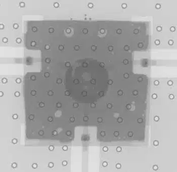
A soldered circulator is shown in Fig. 3, and an X-ray inspection in Fig. 4. validates the soldering process with a satisfactory ratio of missing solder to ground plane.
CONCLUSION
For the first time to the authors knowledge, low-loss circulators using LTCC technology compatible with SMD technology have been produced. Furthermore, they were successfully soldered to a printed circuit board using the conventional SMD transfer process and were measured.
The successful soldering of the circulators on the transfer board was observed via an X-ray observation. The correct operation of both the LTCC compatible SMD transition as well as the circulator designs were verified through the measurement of electromagnetic performance close to those expected.
The two circulators presented here are currently state of the art in terms of insertion loss in Ku band for LTCC circulators, despite the addition of SMD transitions. Both the measured bandwidths at -18dB exceeded the expectations with an increase of almost 80% for the spinel circulator.
Read the full paper:


