source: Denis Zogbi, Paumanok, TTI MarketEye article
Because of Paumanok’s depth and breadth of market and technology data on passive electronic components we have had the great opportunity to participate in the development of many advanced passive component technologies over the past 30 years. It is my observation that the market moves in cycles and that it is time again for the technology to move forward. And while many great words have been written to describe the directional correctness of the high-tech economy; the best four are “better, smaller, faster, cheaper.”
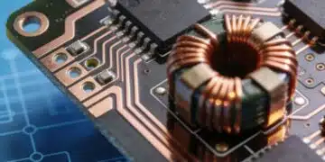
Passive components hold an important key to the future of how technology will improve while becoming smaller. In the past, design engineers looked strictly at the Bill of Materials to produce the “black box.” And were always distracted by the expensive silicon, and noted passives, only because they appeared far, far down the cost list, at the end, with a combined 2.3% of the BOM1. However, today, the realization that the majority of physical space on the printed circuit board is dominated by passive components (with emphasis on ceramic chip capacitors, thick film chip resistors, ceramic chip inductors, and multilayered ferrite beads), is finally becoming a critical area in the next step in moving end-product technology forward2.
Miniaturization Trends
Smaller case size passive components are important developments in helping reduce the physical size of the electronic goods into which they are sold. Those products that have had the greatest impact on driving the development for smaller case size capacitors, resistors and inductors include smartphones, laptop computers, personal digital assistants, digital still and video cameras; and flat panel displays.
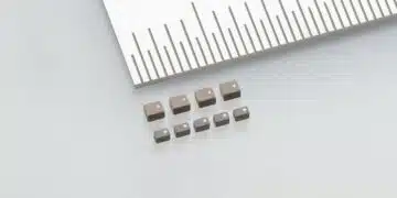
In ceramic capacitors, with emphasis on MLCCs, miniaturization has been dramatic, with global demand switching from the larger 0805 case size parts to the smaller 0603 and 0402 case size parts, and then dropping down to the astonishing 0201 (EIA) case size in 2003, and by 2016 the 01005 had created a firm foothold as the next generation in extremely small electronic components. And now the trend moves forward with the introduction of the 008004 in MLCC thick film chip resistor and in ceramic chip inductor (very cutting edge, very state of the art). But as the discussions around the conference rooms for many of the major brand name OEMs who dominate the high-tech economy, the goal has to be to be able to produce an entire power amplifier or communication module in a 0201 case size. To achieve that goal in the future, to drive the Internet of Everything into the granularity of human existence, the passive components in the design need to provide their function but be invisible, and be as exactly precise in their performance as possible. To achieve that goal, major design houses will have to extend the palette of the materials that they work with; a more expanded view of the periodic table; and expand the processing capabilities of the machines they use to build the products of the future.
Next Generation= Integration and Modularization
In the 1960s, resistor manufacturers such as Vishay Intertechnology, Inc. began to package individual resistors into single-in-line packages (SIP) that housed four to eight individual components. This packaging reduced the cost of placing resistors on a printed circuit board (“conversion cost”).
Soon after that, the component manufacturers realized their ability to make networks on an alumina bridge also meant that they could provide value-added configurations (such as bussed and R2R Ladder circuits for filtering and line-termination). Over time, this concept was enhanced to include thick-film networks of 16 to 32 resistive elements within dual-in-line packages in plastic housings with gull-wing leads for easy surface mounting. The dual-in-line package (DIP) made it possible for resistor manufacturers to integrate different types of passive components, usually chip resistors and ceramic chip capacitors.

In the early 1990s, new developments in passive component configuration were pioneered by companies in the discrete semiconductor industries who successfully used semiconductor manufacturing techniques to manipulate specific raw materials, such as tantalum nitride, chrome silicide, and nickel-chromium, to create layers of resistance. They also used ion-implantation devices to engineer silicon-oxide- and silicon-nitride capacitors; thereby creating complex integrated passive devices (IPDs). Additional silicon manipulation in thin film added transistor functions and circuit protection functions to IPDs. The new thin-film-on-silicon designs began to compete against traditional thick-film DIPs and SIPs for termination and filtering functions, especially in high-frequency applications.
While thin-film IPDs were finding their niche, chip-resistor manufacturers developed the multichip array based on thick-film technology. The multichip array was a low-cost alternative to traditional thick-film SIP products, and it lowered the placement costs on PCBs. The combination of low cost array components, coupled with the added customer savings in conversion costs, caused the array market to grow rapidly, especially in markets where volumetric efficiency was of extreme importance.
Companies that had been making arrays and networks (especially those with multilayer technology) began to realize they could use their manufacturing know-how and technology to produce advanced components and modules. The result was the complex integration of capacitors, resistors, and inductors in low temperature co-fired ceramic (LTCC) substrates.
As a byproduct of this technological advancement, a portion of R&D spending shifted from customers to the component vendors.
LTCC components and modules have been used in automotive applications for some time, especially for engine control. Now, wireless devices represent a new, high-growth opportunity for LTCCs. There are 500 to 1000 passive components in a typical wireless handset, of which about 45% are MLCCs and 25% are chip resistors. Over time, these components gradually have moved from being pick and placed directly on the printed circuit board to appearing inside the modules (power amplifier, communication) instead which has made them harder to count, but what it also means is that modularity is the future and making chipsets smaller is the goal.
Component Integration versus Material Manipulation
Integrated passive components and modules achieve capacitance, resistance and inductance by combining individual components either on or inside the substrate material.
A substantial amount of effort is underway to develop high K and high Q materials that can easily lend themselves to co-firing (for LTCC) or FR4 laminate assembly. This technology is generally described as “integral passive substrate material development”. The makers of FR4 modules see integral passive substrates as a way to get beyond FR4’s two-dimensional (less dense) model. The makers of LTCC modules are interested in integral passive substrates because they offer lower parasitic inductance in the finished module when compared to individual discrete components that have been co-fired.
Component Manufacturers are Smart Too
Companies such as Murata Manufacturing of Japan have moved the technology forward by constantly being a step ahead in MLCC and chip inductor miniaturization. The materials engineering and process control required to successfully produce a 008004 EIA case size component is an enabling technology because they the consistent performance of the components gives a greater lot-to-lot consistency of quality for the module manufacturers. But the discussions always go to the point that at 008004 the component is hardly visible to the eye. This is exactly what the more expensive processes of module manufacturers wanted, but they also know at a certain point, the ability to produce components in a traditional sense will go from individual components to sputtering and etching and the use of semiconductor equipment to process important circuit functions once accomplished by individual discrete components.
Forecasts
The impact of component-modularization could be as great as the recent movement of manufacturing away from OEMs to the CEMs. Component modularization offers component vendors substantial value-added opportunities. As pre-fabricated modules incorporate increasingly larger percentages of passive component circuitry module vendors will take some power away from the mass assembly houses in the interest of increasing the throughput of manufacturing. Individual component manufacturers with grand investments in massive economies of scale to produce capacitors and resistors, will realize that by working with raw materials suppliers to develop the highest quality ceramics and metals, and the process technology required to create thin sheets and layers, they can continue to move the technology forward by creating increasingly smaller components. But at some point the component manufacturer will have to invest in a combination of disciplines and technologies, including ceramic multilayered stacking, thin film sputtering, photolithography, and co-firing to achieve continued ultra-small modularization to move the high-tech economy forward in its attempt to be “better, smaller, faster, cheaper.”
1 (My friend and mentor- Dr. Felix Zandman once walked me through the 72 step process to build tantalum capacitors in his factory in Dimona, Israel, and I stated, “It’s hard to believe that something this complicated produces a part that costs only $0.035 a piece, and Felix said “And the whole process took years to master.”)
2 Printed circuit boards also contain a variety of additional passive electronic components such as metal oxide varistors, PTC and NTC thermistors, SMD gas tubes, a variety of filters and EMC compatability components representing a proverbial “soup” of electronic materials.


