





Most MLCC ceramic capacitors are relatively inexpensive, but when a capacitor fails in service, the consequences may be anything from a slight change in a video image to the complete failure of a system. So their testing is important. Tom Adams, consultant to Nordson SONOSCAN, USA published an article in electronicsforu.com that explains basic principles and defect analysis methods.
Multi-layer ceramic chip capacitors (MLCCs) work by storing energy and releasing it when it is needed. They consist of stacks having alternating layers of a thin metal electrode and a thicker ceramic dielectric, or insulator. Because of their layered structure, MLCCs are ideal for inspection by an acoustic micro imaging (AMI) tool.
This tool sends a pulse of ultrasound into the surface of the MLCC and receives and analyses the return echoes from within the part. It performs this task up to 30,000 times per second while scanning across the MLCC just above its surface. The end result is an acoustic image of the MLCC’s interior, including structural defects.
The echoes come only from material interfaces—where a material is in contact with another material. In a semiconductor device, this might be the interface between mould compound and silicon, which would give a strong echo because the acoustic impedance (acoustic velocity x density) values of the two materials are so different.
The operator of an AMI tool examining an IC device may be dealing with features at a few to several depths, but even small low-voltage MLCCs may have hundreds of alternating layers of ceramic and metal. At interfaces between solid materials, part of the pulse is reflected and part transmitted through the interface. If the acoustic impedances of ceramic and metal were very different from each other, a launched pulse could be completely attenuated after the first few layers. But the acoustic impedances of the ceramic and metal in MLCCs are slightly different, so echoes can be pulsed into and reflected from the bottom layer of the MLCC, even if there are hundreds of layers.
Electrical failure of an MLCC may begin with an air inclusion trapped during fabrication of the component. The inclusions can broadly be separated into two types: voids and delaminations. Voids are found in the dielectric and are spherical or almost any other shape, but are typically more three-dimensional than delaminations. Delaminations are typically flat air pockets between the dielectric and an electrode.
Under mechanical and electrical stresses of thermal cycling, both voids and delaminations are capable of expanding to cause a dielectric breakdown. Failure occurs when a conductive pathway is created through the dielectric between two electrode layers and becomes a leakage pathway or a short circuit.
It is beneficial, then, to find any voids or delaminations or other air gaps in an MLCC before it is mounted onto a board (or even after it is mounted, if necessary). Whether the AMI tool is imaging a single MLCC or whole trays of MLCCs, the imaging process follows this sequence:
- A pulse is launched by the transducer and travels 3mm or so through a water column to a precise x-y location on the surface of the MLCC.
- Part of the pulse is reflected by the interface between the water and the MLCC’s surface back to the transducer, where its travel time in nanoseconds is recorded to provide a record of the precise distance between the transducer and the MLCC.
- The other portion of the pulse crosses the interface and travels into the ceramic-metal layers comprising the capacitor, where it is slightly reflected at each material interface.
- Within the capacitor, if the pulse strikes the top surface of an air-filled void or delamination, virtually all of the pulse is reflected to the transducer where its amplitude, arrival time, and sometimes other properties are measured. The pixel made from it will be bright white or bright red, the two colours typically used to indicate a reflection of maximum amplitude.
- If the pulse strikes no solid-to-air interface, it will continue on to the bottom of the capacitor and be reflected from there back to the transducer. From crossing so many minimally reflective interfaces, both going and returning, the pulse/echo will have lost energy.
Fig. 1 shows the acoustic image of an MLCC having a large internal defect. A pulse was launched into each of the thousands of x-y locations that make up the whole acoustic image, and a colour from the colour map at left was assigned to each location. Green pixels represent the dieletric-electrode stacks, while red is the packaging around them.
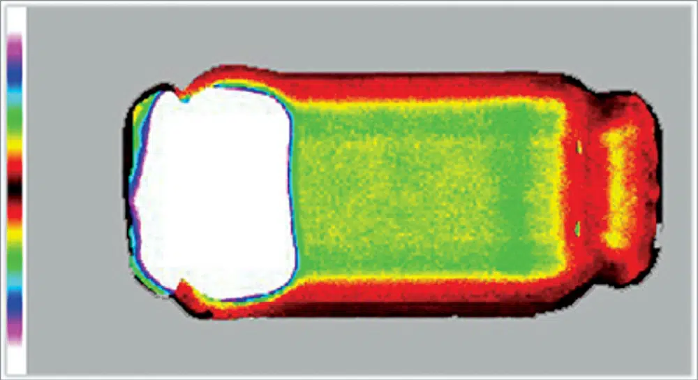
Solid white in the area at left represents echoes having the highest amplitude. This area is the interface between the electrode and the air in the delamination. None of the ultrasonic pulses traveled deeper in this area because ultrasound at these frequencies will not travel through air, even if the air is only a tiny fraction of a micron in thickness.
A small portion of a tray of MLCCs that have been imaged acoustically is shown in Fig. 2. Echoes were collected simultaneously from all depths within the capacitors to make this image. The result is that all air-gap defects are visible, but there is no information in this image to determine their order to evaluate their depth. So, acoustic cross-sections can be made or a separate image can be made of each step.
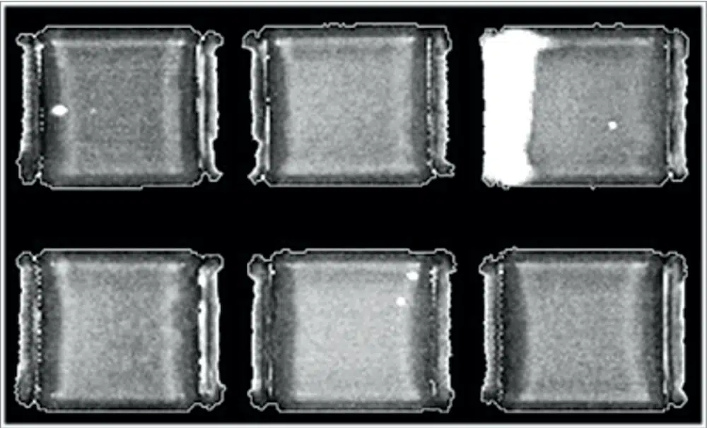
Three of the six capacitors have air-type defects. Four of the defects are small voids, but the fifth is a massive delamination incorporating an unknown number of layers within the capacitor. The two capacitors in this image having only small defects may at this point be electrically viable, but the fifth capacitor almost certainly is not.
Large quantities of MLCCs in trays are imaged rapidly by automated AMI tools. MLCCs identified as harbouring defects are removed before a lot of the capacitors is used in assembly.
Fig. 3 shows the acoustic images of two (out of six) levels that were imaged in the same MLCC. To make a separate acoustic image from each depth, a gate was set telling the echo receiver in the transducer to use the echoes whose arrival times indicate that they originated between depth A and depth B to make a separate image.
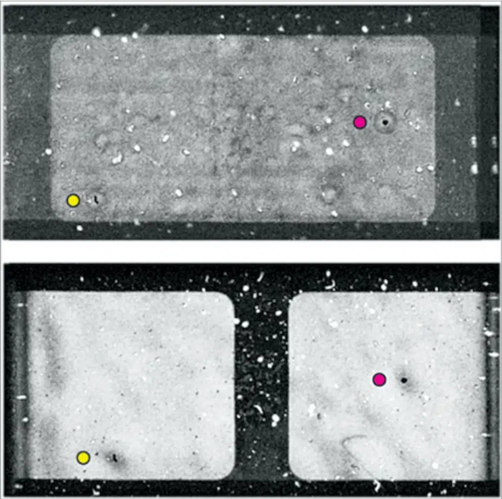
The echoes that arrive in the first sixth of the total time span are assigned to gate 1 and displayed as a separate image. Those in the next sixth are assigned to gate 2, and so on. The result is an image sequence showing the interior of the capacitor in six evenly thick slices. If needed, there can be hundred or more slices, and they can have different thicknesses, ranging down to extremely thin. When it is necessary to know what features exist at specific depths within a component, this is a very useful imaging mode.
The plates in each of the two stacks in this capacitor are staggered. If the two plates in gate 4 (at the bottom) were pushed together, they would have the same orientation as the plates in gate 3 (at top).
Overall, this capacitor has too many voids to be considered for assembly. Most of the voids are seen in only one of the two images, but a few that probably lie close to or at the boundary between the two plates can be seen in both the images.
There are also a few darker features that are the acoustic shadows of voids or delaminations, which lie above a given gate. Two of them are marked by red and green dots. The two marked items must lie above, in gates 1 or 2.
Here is what has happened: a pulse from the transducer strikes a feature in gate 1 or gate 2 and is reflected to the transducer, thereby ‘using up’ the echo from that x-y position. No ultrasound travels deeper at that position, so when the transducer is collecting echoes from gates 3 and 4, there is nothing at that x-y position, which remains a dark pixel.
There are about a dozen other AMI tool imaging modes that can be used to image MLCCs. One imaging mode non-destructively cross-sections through as many vertical planes in an MLCC as desired. Another imaging mode shows internal features in three dimensions.
Another mode images the flatness of the MLCC’s surface, and yet another mode images its internal features at single ultrasonic frequencies.
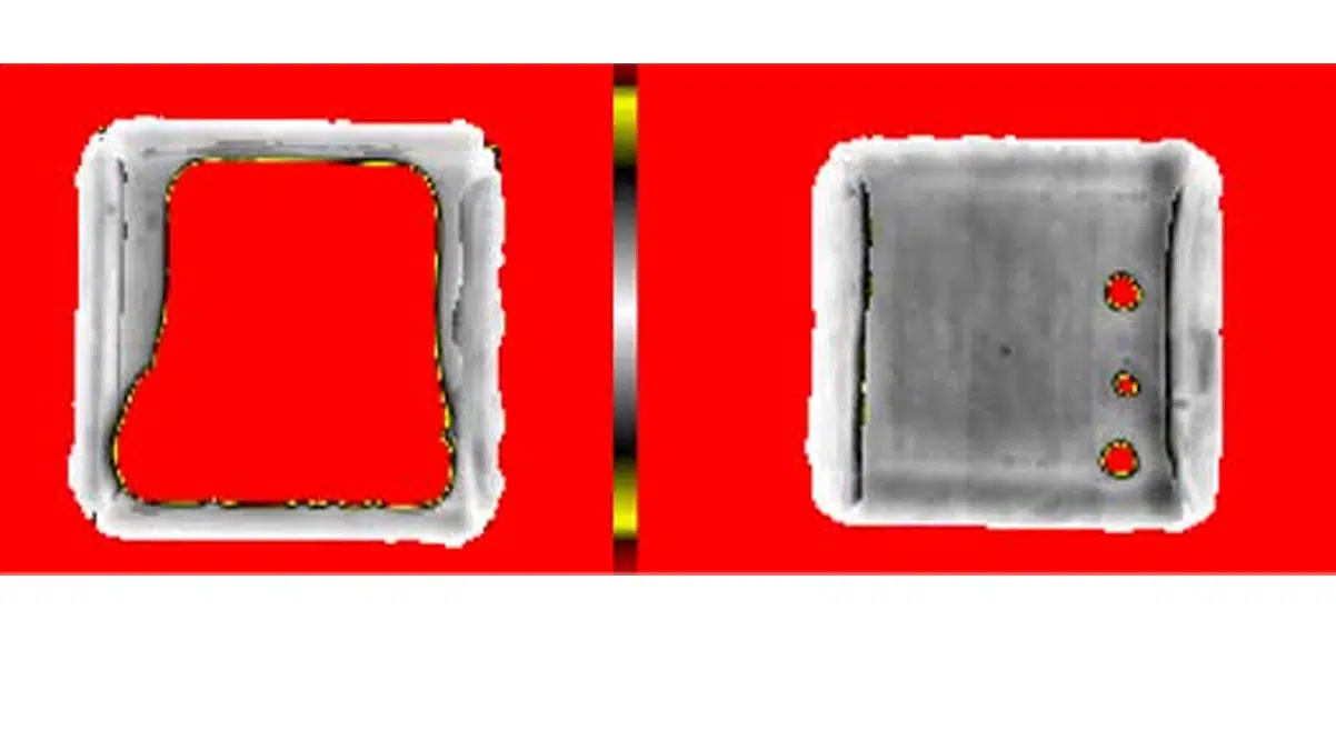
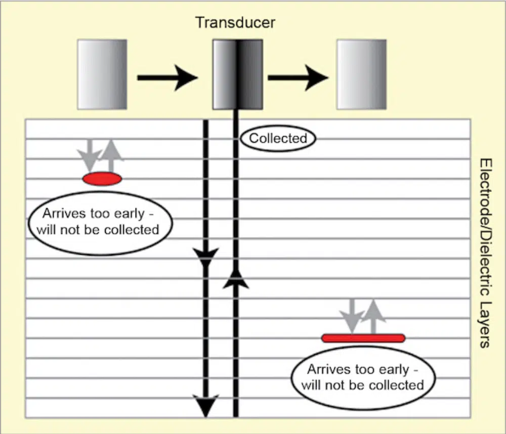
There is also a method, especially useful for high-power MLCCs, that images all internal features capable of blocking ultrasound as acoustic shadows, as shown in Fig. 3. The detailed operation is shown in Fig. 4.
This method collects an echo only when a pulse has traveled to the bottom of the capacitor and back without encountering an imageable feature—as seen in the centre of the figure. The echo will be attenuated somewhat but will arrive in the gate assigned to it at precisely the right time. The acoustic image will show a grayish pixel at this x-y location.
At left in Fig. 4 is the path of a pulse that encountered a rounded void at a shallow depth. Ultrasound that was not scattered by the sloping sides of the void will be reflected in the direction of the transducer. But since the distance is less, it arrives far too early and is not collected. But no ultrasound will reach the bottom directly beneath the void. Areas around it will be reflected from the bottom and create a grayish pixel. In the acoustic image, then, the oval pulse will be black (no echoes received at the right time) but surrounded by grayish pixels.
The flat delamination at lower right has essentially the same fate. When a pulse strikes it, the ultrasound is reflected, but it arrives too soon to be in the proper gate. Like the void, it becomes a black acoustic shadow in a gray field.
The whole acoustic image will therefore show voids and delaminations as dark features—acoustic shadows. Since voids and delaminations are harmful at any depth, any capacitor exhibiting dark features will be discarded. Since the mere presence of defects is enough to disqualify such capacitors, the defect’s depth is unimportant.