






Passive Components Blog
No Result
View All Result
  • Home
  • News
    • All
    • Aerospace & Defence
    • Antenna
    • Applications
    • Automotive
    • Capacitors
    • Circuit Protection Devices
    • electro-mechanical news
    • Filters
    • Fuses
    • Inductors
    • Industrial
    • Integrated Passives
    • inter-connect news
    • Market & Supply Chain
    • Market Insights
    • Medical
    • Modelling and Simulation
    • New Materials & Supply
    • New Technologies
    • Non-linear Passives
    • Optoelectronics and Isolation
    • Oscillators
    • Passive Sensors News
    • Resistors
    • RF & Microwave
    • Telecommunication
    • Weekly Digest
    Bourns CSS4C-1216 four-terminal metal-strip current sense resistor for high-current Kelvin measurement

    Bourns Extends 1216 Kelvin Current Sense Resistors

    Modelithics COMPLETE+3D Library v26.3 for Ansys HFSS with RF passive component and 3D electromagnetic simulation models

    Modelithics COMPLETE+3D v26.3 Expands HFSS RF Models

    Samsung Electro-Mechanics low-profile and embedded MLCCs for compact PCB and power-delivery applications

    Samsung Low-Profile and Embedded MLCCs for Compact Devices

    Wk 36 Electronics Supply Chain Digest

    Bourns Adds ACXX57SQ Air Coil Inductors for RF Design

    Samsung Electro-Mechanics MLCC capacitor solutions for high-voltage converter snubbing and GPU power delivery

    Samsung MLCC Options for 1 MW AI Rack Power

    Frenetic planar ER transformer simulation for a 5 kW 800 V-to-50 V PSFB converter, showing low-profile core geometry and high-current planar winding arrangement

    5 kW 800 V-to-50 V PSFB Transformer Design for Data Centers

    Samtec 100-CM 1.0 mm vertical solderless compression-mount 50 ohm RF PCB connector

    Samtec 100-CM 1.0 mm RF Connectors Extend to 120 GHz

    Exxelia PM film capacitor and passive-component technologies for BepiColombo space electronics

    Exxelia Passive Components Support BepiColombo Mission

    Trending Tags

    • Ripple Current
    • RF
    • Leakage Current
    • Tantalum vs Ceramic
    • Snubber
    • Low ESR
    • Feedthrough
    • Derating
    • Dielectric Constant
    • New Products
    • Market Reports
  • Knowledge Blog
  • Dossiers
    • AI Hardware Dossier
    • Automotive Dossier
    • Industrial Robotics Dossier
    • Power Converter Dossier
    • Capacitor Dossier
    • Resistor Dossier
    • Inductor Dossier
    • Circuit Protection Dossier
  • Suppliers
    • Who is Who
  • PCNS
    • PCNS 2025
    • PCNS 2023
    • PCNS 2021
    • PCNS 2019
    • PCNS 2017
  • Events
  • Home
  • News
    • All
    • Aerospace & Defence
    • Antenna
    • Applications
    • Automotive
    • Capacitors
    • Circuit Protection Devices
    • electro-mechanical news
    • Filters
    • Fuses
    • Inductors
    • Industrial
    • Integrated Passives
    • inter-connect news
    • Market & Supply Chain
    • Market Insights
    • Medical
    • Modelling and Simulation
    • New Materials & Supply
    • New Technologies
    • Non-linear Passives
    • Optoelectronics and Isolation
    • Oscillators
    • Passive Sensors News
    • Resistors
    • RF & Microwave
    • Telecommunication
    • Weekly Digest
    Bourns CSS4C-1216 four-terminal metal-strip current sense resistor for high-current Kelvin measurement

    Bourns Extends 1216 Kelvin Current Sense Resistors

    Modelithics COMPLETE+3D Library v26.3 for Ansys HFSS with RF passive component and 3D electromagnetic simulation models

    Modelithics COMPLETE+3D v26.3 Expands HFSS RF Models

    Samsung Electro-Mechanics low-profile and embedded MLCCs for compact PCB and power-delivery applications

    Samsung Low-Profile and Embedded MLCCs for Compact Devices

    Wk 36 Electronics Supply Chain Digest

    Bourns Adds ACXX57SQ Air Coil Inductors for RF Design

    Samsung Electro-Mechanics MLCC capacitor solutions for high-voltage converter snubbing and GPU power delivery

    Samsung MLCC Options for 1 MW AI Rack Power

    Frenetic planar ER transformer simulation for a 5 kW 800 V-to-50 V PSFB converter, showing low-profile core geometry and high-current planar winding arrangement

    5 kW 800 V-to-50 V PSFB Transformer Design for Data Centers

    Samtec 100-CM 1.0 mm vertical solderless compression-mount 50 ohm RF PCB connector

    Samtec 100-CM 1.0 mm RF Connectors Extend to 120 GHz

    Exxelia PM film capacitor and passive-component technologies for BepiColombo space electronics

    Exxelia Passive Components Support BepiColombo Mission

    Trending Tags

    • Ripple Current
    • RF
    • Leakage Current
    • Tantalum vs Ceramic
    • Snubber
    • Low ESR
    • Feedthrough
    • Derating
    • Dielectric Constant
    • New Products
    • Market Reports
  • Knowledge Blog
  • Dossiers
    • AI Hardware Dossier
    • Automotive Dossier
    • Industrial Robotics Dossier
    • Power Converter Dossier
    • Capacitor Dossier
    • Resistor Dossier
    • Inductor Dossier
    • Circuit Protection Dossier
  • Suppliers
    • Who is Who
  • PCNS
    • PCNS 2025
    • PCNS 2023
    • PCNS 2021
    • PCNS 2019
    • PCNS 2017
  • Events
No Result
View All Result
Passive Components Blog
No Result
View All Result

Designing of Analog-to-Digital Input Drive of RF Converters

14.4.2020
Reading Time: 8 mins read
A A

Understanding the input drive and full-scale range trade-offs in ADCs can be vital when designing analog receiver front ends, Rob Reeder, applications engineer, high-speed data converters, Texas Instruments published his article in Electronic Products Magazine.

Let’s face it: analog-to-digital converters (ADCs) operate differently. Their analog inputs are voltage-input-sensitive devices that leave radio-frequency (RF) engineers scratching their heads about how to match the ADC to the analog inputs.

RelatedPosts

Bourns Extends 1216 Kelvin Current Sense Resistors

Modelithics COMPLETE+3D v26.3 Expands HFSS RF Models

Samsung Low-Profile and Embedded MLCCs for Compact Devices

Adding to this confusion, analog input interfaces are typically differential by nature and host a time-varying type of input impedance as the internal sampling switch opens and closes at the speed of light. This input impedance is thought to be a real resistive value across the ADC’s input bandwidth, but when plotted on a Smith chart, the trace curve just goes around and around.

In this article, I’ll look at some of the details related to analog input trade-offs, and how to properly deduce the ADC’s full-scale range in reference to the analog input network in dBm.

It’s all about headroom

Long ago, high-speed ADCs were designed on process nodes that supported voltage swings as large as 10-Vpp full scale.

They were even single-ended. Setting the ADC’s reference gave you some flexibility to make the full-scale range unipolar or bipolar.

Today, the process nodes are small – 65 nm or less – and the ADC’s internal analog input front end is biased at <2 V. This makes for significantly lower headroom, which can become a challenge when signal-chain designs need to interface with a 1- or 2-Vpp full-scale range, where the RF stops and the ADC begins.

Today, most high-speed ADCs employ differential inputs. This implies that you only have one-fourth the signal swing to wrap around the common-mode voltage (VCM) bias, or each analog input handles one-half the swing. Fig. 1 illustrates single-ended vs. differential signal properties and definitions

TI-RF-converter-Figure1-small
Fig. 1: Single-ended vs. differential analog input signals

The ADC’s analog input VCM is important and needs to be satisfied by the external input network front end; otherwise, the device will have other performance challenges.

By dividing up the signal swing differentially, this interface enables you to maintain higher voltage levels across the full-scale range (that is, 1 or 2 Vpp); therefore, the differential nature of the analog input enables a smaller process node.

Full-scale trade-offs

Some ADCs are flexible and dedicate a few (out of the few thousand) serial peripheral Interface (SPI) registers in order to change the full-scale swing. Keep in mind that a design with a larger full-scale range generally yields a better signal-to-noise ratio (SNR). But better SNR performance usually decreases the harmonic performance of the spurious free dynamic range (SFDR).

The SNR increases because the signal swing can be larger now, assuming that the noise stays constant. Conversely, a smaller full-scale range enables better SFDR (HD2 and HD3); however, there is a slight sacrifice in SNR. See Figs. 2 and 3to understand these trade-offs.

TI-RF-converter-Figure2-small
Fig. 2: Minimum full-scale value (430-mVpp) = SFDR increase

As shown in Fig. 2, the input full-scale range changed from a default value of 800 mVpp to 430 mVpp. This reflects a slight increase in SFDR or HD2 and HD3. The input full-scale value changing from the default 800 mVpp to 1.0 Vpp yields a slight increase in SNR, as shown in Fig. 3. Notice the HD2 and HD3 decrease in Fig. 3 vs. Fig. 2.

TI-RF-converter-Figure3-small
Fig. 3: Maximum full-scale value (1.0-Vpp) = SNR increase

In either case, you can “dial in” the best AC performance for your application by optimizing the full-scale value.

Other SPI registers allow you to change the input impedance, possibly halving or doubling the input impedance on the differential inputs. This means that you can optimize the “matching” network when designing the front end. The input full-scale range will once again change in value. Not all ADCs offer these features, but some do, which is easier than changing the front-end circuitry to accommodate different applications or adding additional components to the front-end network.

Full-scale breakdown

Let’s go through an example that illustrates the trade-offs involved when designing a high-speed matching network to the ADC. Baluns and front-end networks will add loss and additional noise figure to the overall signal chain, so it is pertinent to understand the input-drive trade-offs during the design and optimize the full-scale value. The input drive defines the amount of signal (in dBm) required to drive the converter at a full-scale range in front of the interface network – in this case, a passive balun network.

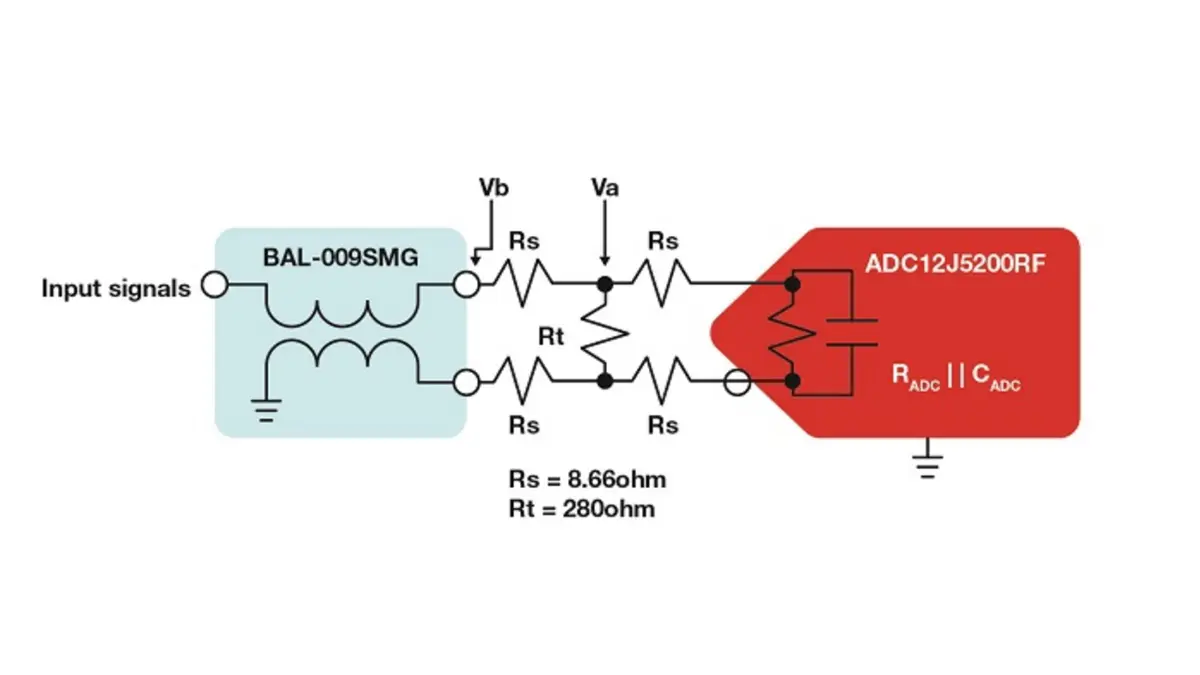
In the example, the ADC is the RF-sampling, 12-bit ADC12DJ5200RF from Texas Instruments and the balun is the BAL-0009SMG from Marki Microwave. A front-end resistive network interfaces the balun’s differential outputs to the ADC differential inputs. See Fig. 4.

TI-RF-converter-Figure4-small
Fig. 4: Example front-end network

Let’s do some calculations next. If you don’t have a dBm calculator handy, I recommend downloading the latest graphing calculator app to your phone.

The ADC12DJ5200RF has a default analog input full-scale range of 800 mVpp (Vfs) with a 100-Ω (RADC) differential load internally that is calculated in terms of dBm (Equation 1):

PADC= 10*log((Vfs/2/sqrt(2))2/Radc/1e03) or 10*log((800m/2/sqrt(2))2/100/1e-3) = -0.97 dBm (1)

Since the input network is differential, it can become a little difficult to crunch through the numbers. But by using the single-ended approach, the full-scale voltage at the input of the ADC has a value of 400 mVpp (Vfs/2) or -3.97 dBm.

By using a front-end resistive network as described above, you can calculate the voltage dividers to understand the losses required to achieve a 400-mVpp (Vfs/2) full-scale value.

RADC/2 = 50 Ω and Rs form a resistive divider or Va = (Vfs/2)*(((RADC/2)+Rs)/RADC) = 0.47 V, which gives you a single-ended voltage input at Rs and Rt.

Now, let’s calculate the single-ended voltage at the balun output (Equation 2):

Vb = Va*(((((RADC/2)+Rs)||(Rt/2))+Rs)/(((RADC /2)+Rs)||(Rt/2))) = 0.57 V                (2)

You can make this single-ended voltage a differential voltage or 2*Vb or 1.13 V = Vdiffbo. The power at the balun’s output is then expressed as Equation 3:

Pbo = 10*log((((Vdiffbo/2/sqrt(2))2)/RADC)/1e-3) = 2.06 dBm                       (3)

Now for the fun part: Either consult the data sheet of the prospective balun or measure the balun on your nearest four-port vector network analyzer and take an SDS21. This will yield a single-ended-to-differential measurement and provide the correct insertion loss across the balun. In this example, measuring the BAL-0009SMG yields a loss of 4.2 dB at 1 GHz. See Fig.

TI-RF-converter-Figure5-small
Fig. 5: SDS21 insertion loss plot of the Marki Microwave BAL-0009SMG balun

Adding the balun losses to the output power found at the balun’s output (resistive network loss) determines what the input drive is: 2.06 + 4.2 or +6.26 dBm; +6.26 dBm is the required input amplitude required to drive the analog input signal on the primary of the balun to the full-scale range of the ADC.

Therefore, the total losses from top to bottom are 6.26 + 0.97, or a 7.26-dBm loss. Remember the PADC equation (with the result of -0.97 dBm) to achieve the full-scale value? Add that result back in, too.

A quick note on noise figure: When designing an analog receiver chain, the loss in the balun and front-end network counts as well. For this case, the noise-figure addition will be the loss found or 6.26 dBm, which is a value of 1.3 Vpp vs. the default full-scale value of 800 mVpp. This means 20*log(1.3/0.8) = 4.22 dB of additional noise figure in the receiver signal chain.

Now, let’s take a different approach: measuring it in the lab with the ADC12DJ5200RF evaluation module. Using the signal generator, dial in the output level until the ADC is very near the full-scale value at 1 GHz. In this case, the input full-scale value was +6.3 dBm from the signal generator reading. Keep in mind that balun variance and cable/connector losses can cause some differences. See Fig. 6.

TI-RF-converter-Figure6-small
Fig. 6: High Speed Data Converter Pro fast Fourier transform plot showing an unfiltered intermediate frequency of 1 GHz at -0.01 dBFS

Conclusion

Understanding the input drive and full-scale range trade-offs in ADCs can be vital when designing analog receiver front ends. The quick method given here for analyzing the front end should help keep trade-offs well within range. If you have any questions or feedback on this analysis, please comment below.

The author would like to dedicate this article to his mentors: James Bobis and Walt Kester.

Related

Source: Electronic Products Magazine, TI

Recent Posts

Bourns Adds ACXX57SQ Air Coil Inductors for RF Design

18.9.2026
6
Frenetic planar ER transformer simulation for a 5 kW 800 V-to-50 V PSFB converter, showing low-profile core geometry and high-current planar winding arrangement

5 kW 800 V-to-50 V PSFB Transformer Design for Data Centers

18.9.2026
18

KYOCERA AVX Adds 0201 C0G RF MLCCs to KGU Ultra-Low-ESR Capacitor Series

3.9.2026
56

Modelithics COMPLETE v26.4 Expands RF Passive Models for Keysight ADS

28.8.2026
18

Vishay IFBT SMT Flyback Transformers Target PoE and Isolated DC/DC Designs up to 30 W

28.8.2026
28

Current-Dependent Inductors: Using Non-Linear Inductance in Buck Converters and PFC Stages

24.8.2026
57

Current Sense Transformers: Ferrite vs Nanocrystalline Cores for Accurate Current Measurement

5.8.2026
182

Bourns Introduces LTCC Band Pass Filters for 5G C‑Band RF Front‑End Designs

29.7.2026
51

Bourns Introduces LTCC GNSS L‑Band Diplexer for Compact RF Front Ends

24.7.2026
56

Upcoming Events

Sep 29
16:00 - 17:00 CEST

Cybersecurity 2026

Sep 30
15:00 - 16:00 CEST

Positronic Space and Military Connectors

Oct 14
17:00 - 18:00 CEST

Live Demo! Discover KYOCERA AVX Antenna Integrator Studio (AIS)

View Calendar

Popular Posts

  • Buck Converter Design and Calculation

    0 shares
    Share 0 Tweet 0
  • LLC Resonant Converter Design and Calculation

    0 shares
    Share 0 Tweet 0
  • Boost Converter Design and Calculation

    0 shares
    Share 0 Tweet 0
  • Flyback Converter Design and Calculation

    0 shares
    Share 0 Tweet 0
  • Capacitor Charging and Discharging

    0 shares
    Share 0 Tweet 0
  • Resistor Symbols

    0 shares
    Share 0 Tweet 0
  • MLCC and Ceramic Capacitors

    0 shares
    Share 0 Tweet 0
  • Thermistors Basics, NTC and PTC Thermistors

    0 shares
    Share 0 Tweet 0
  • Audio Capacitors: Choosing Capacitors for Crossover Circuits

    0 shares
    Share 0 Tweet 0
  • Ohm’s Law Answers Your Questions

    0 shares
    Share 0 Tweet 0

Newsletter Subscription


Passive Components Blog

© 2015–2026
All rights reserved

  • Home
  • Privacy Policy
  • EPCI Membership & Advertisement
  • About

No Result
View All Result
  • Home
  • Knowledge Blog
  • Dossiers
  • PCNS

© 2015–2026
All rights reserved