


This article provides an introduction into electromagnetic shielding, elaborates on function of the housing shielding and its effectiveness. The post is based on Würth Elektronik‘s “Reference Guide ABC of Shielding” that can be ordered from WE website here. Published under permission from Würth Elektronik.
The relevance of developing an electronic product that is electro-magnetic compliant (EMC compliant) is increasing.
In the past, EMC was often seen as a discipline for the fulfilment of normative requirements. Now it has established itself as an important challenge for the basis of the functionality of products.
It is essential to understand how the interrelationships between electronics and the housing influence the EMC parameters and thus affect product quality. These parameters include the housing shielding effectiveness, the opening size, the housing material, the peripheral cables, and the ground.
Relationship Between System Components And Effectiveness Of Shielding
Any electrical or electronic device is a potential source of electromagnetic interference. The devices generate electromagnetic energy in certain frequency ranges. Other electromagnetically sensitive devices operating in these frequency ranges can be impaired in their function, by this potential source of interference. In addition, electrical or electronic products must be resistant to external electromagnetic interference such as electrostatic discharge (ESD), electromagnetic fields, and power line interference. This unwanted interference emission, as well as insufficient immunity to interference, results from:
- Digital switching and non-linearities in semiconductor devices
- Incorrect circuit and layout design of the electronics
- Incorrect system or device design
- Insufficient shielding properties of the housing
Designing for EMC compliance is therefore an interdisciplinary field. All four points mentioned above influence each other and must be considered in their interdependencies for a professional device design.
Shielding is often expensive and difficult to implement due to many factors, such as aesthetics, tool costs, weight, and other factors. A decision on whether or not to use shielding should be made as early as possible in the project.
The product developer should be able to roughly estimate the fields generated by the electron-ics and also estimate the immunity of the circuit to the required interference phenomena. If no rough estimation can be made, pre-compliance measurements should be carried out to esti-mate the EMC behavior of the circuit. If the product shows EMC weaknesses and the electronics cannot be improved, shielding is essential. In general, it can be said:
- If the radiation of the electronics in differential mode exceeds the limit values, shielding is essential.
- If increased immunity to interference is required for industrial or medical applications, shield-ing is essential.
- If the circuit requires several interfaces with shielded cables, shielding is probably essential.
- If the layout on the outer layers allows for shielding, a metal ground plane (copper plane) may be sufficient; then consider shielding only for critical circuit areas, if necessary.
An EMC compliant system design ensures that the electronic system components, such as assemblies, cables, interfaces, and operating elements, are integrated into the housing in such a way that:
- No negative EMC interactions occur between the system components.
- The techniques and conditions specified for product design can be implemented in the best possible way.
- Electromagnetic and other normative requirements, like safety requirements for the product, are fulfilled.
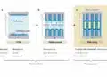
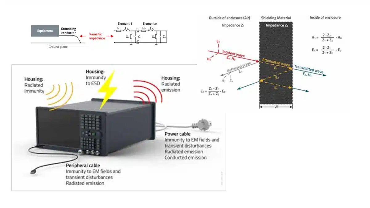
The system engineer and designer must consider the detailed electromagnetic properties of the system components to design an effective but not overdesigned enclosure. These properties relate not only to the emission of electromagnetic energy but also to the required immunity of the product to external electromagnetic phenomena (Figure 1.).
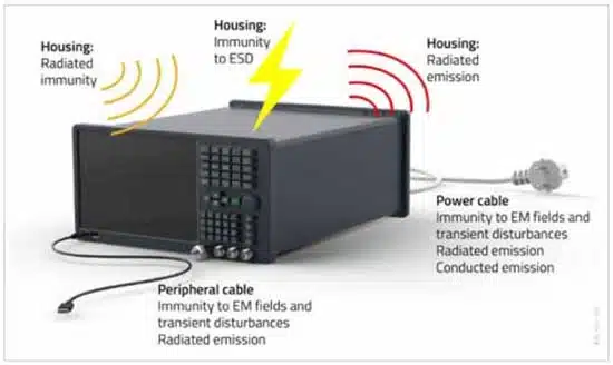
To fulfill these requirements, the housing must meet the following conditions:
- Reference ground for the electronic components inside the product (depending on the ground concept)
- Reference ground for filters to attenuate conducted or radiated interference like RF noise and transients, via cables
- From the device to the outside (interference emission)
- From the outside into the device (interference immunity)
- Shielding and/or insulation against electrostatic discharges
- Shielding of electromagnetic fields
- Radiated from the internal electronics of the device (interference emission)
- Radiated on the device from outside (interference immunity)
Ground systems
There are two main reasons for grounding the equipment. One reason is the safety aspect, and the second reason is to reduce EMC effects caused by electromagnetic fields or other forms of interference. For EMC, the internal ground system should ideally provide a zero-impedance path for all signals for which it serves as a reference. In this case, the signal currents from different circuits or components connected to ground could return to their respective sources without causing unwanted coupling between circuits or between neighboring components. Many EMC problems occur because designers assume an ideal ground rather than considering the actual characteristics of the ground system.
Each section of a conductor and each metal housing part, has properties such as resistance, capacitance, and inductance. Shields, protective conductors, grounding bars, sheet metal walls – all conductors have these properties. These properties of the conductor section are a function of its geometrical and material-specific properties. The impedance of the conductor is then calculated from the resistance (skin effect considered), capacitance, inductance, and frequency of the cur-rent flowing through the conductor.
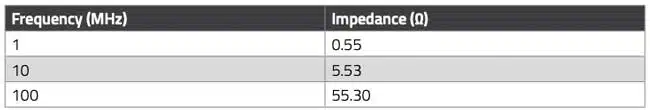
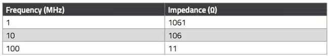
Table 1. shows the impedance of straight, round wires for different wire thicknesses (d) and lengths (l) as a function of frequency. Typical impedances of ground planes, e.g., housing plates, with different thicknesses (t) are given in Table 2. for comparison. The values in Table 2. are given according to the standardized sheet resistance measurement. Sheet resistance is the resistance of a square piece of a thin material with contacts on two opposite sides of the square. It is a measurement of the electrical resistance of thin films that are uniform in thickness, and commonly used to characterize materials.

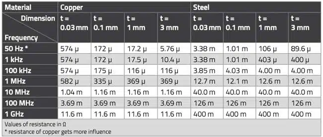
Note that for typical wire lengths, the impedances of the ground planes are several orders of magnitude lower than those of a round wire. Nevertheless, it should be noted that the impedance of both round wires and ground planes increases with increasing frequency and rises significantly at higher frequencies, so that an “ideal” reference ground can no longer be assumed!
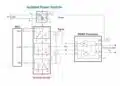
A common situation is that of a ground cable (current or signal) running near a ground plane. This situation, with the corresponding equivalent circuit diagram, is shown in Figure 2. The conductance G can be neglected in practice. R is the AC resistance of the copper when taking the skin effect into account, L is the inductance of the conductor, and C is the parasitic capacitance of the conductor arrangement in relation to the ground plane.
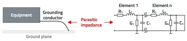
The grounding conductor over the ground plane is terminated at the end and thus works partly as a transmission line and partly as a monopole, depending on the relation between the electri-cal length of the wire and the wave length. This is why the equivalent diagram has a short at the end.
At very low frequencies (typ. <10 kHz) the effects of the resistive part of the impedance are dominant. At higher frequencies, the influences of the reactive resistances of the inductive and capacitive impedance components increase significantly, and the skin effect must be taken into account in addition to the inductance. The following are some calculation examples.
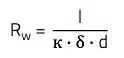
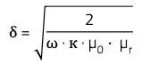
Calculation of the resistance with skin effect:
The alternating current resistance Rw of a conductor under consideration of the skin effect is calculated approximately with:
and
where,
- Rw: Alternating current resistance in Ω
- l: Length of the conductor in m
- к: Specific conductivity in S/m
- δ: Current penetration depth through skin effect in m
- d: Diameter of the conductor in m
- ω: Angular frequency of the current (w = 2 · p · f)
- f: Frequency of the current in Hz
- µ0: Constant of the permeability, 1.257 · 10-6 Vs/Am
- µr: Permeability of the conductor material (without unit!)
Example:
- Frequency: 1 MHz
- Copper wire, length l = 0.5 m, d = 1 mm
- к = 56 · 106 S/m
- µr = 0.99999 this means, approx. = 1
gives: δ = 67.11 µm and Rw = 0.13 Ω the DC-resistance of the wire is only 42 mΩ. At a frequency of 100 MHz the wire already has an alternating current resistance of 1.3 Ω.
Calculation of the inductance L and the impedance XL:
The inductance L of a conductor parallel to the conducting plane is calculated approximately as follows:
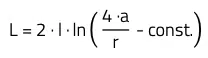
where,
- Precondition: 2a < l
- L: Inductance in nH
- l: Length of the wire in cm
- r: Diameter of the wire in mm
- a: Distance between wire and ground plane in mm
- const.: 0.5 for f > 1 MHz, const.: 0.75 for f < 1 MHz
Example:
- l= 0.5 m
- r = 1 mm
- a = 1 mm
for f > 1 MHz we get: L = 125.276 nH
Calculation of the capacitance C and the impedance XC:
The capacitance C of a conductor parallel to the conducting plane is calculated approximately with:
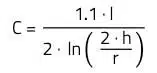
where,
- C: Capacitance in pF
- r: Radius of the wire in mm
- l: Length of the wire in m
- h: Distance between wire and ground plane in mm
Example:
- r=1 mm
- l= 0.5 m
- h = 3 mm
gives C = 0.15pF
The comparison of the impedance shares shows that inductance has the greatest influence on the total impedance in the higher frequency range above 20 MHz. The parasitic capacitance and the parasitic inductance together act like a low-pass filter that only conduct low frequencies towards ground. It goes without saying that such connections are useless as ground reference. Shielding and grounding are complementary practices. Shielding provides not only the shielding effect against electromagnetic fields but also a clean ground reference point for filters – a necessity without which no filter can perform its function.
Function of the housing shielding
The shielding effect of enclosures is based on electromagnetic damping by a conductive barrier of infinite extension, which means that the ideal enclosure should be a “box” completely closed around the electronic circuit. This is counteracted by design requirements that provide these boxes with openings, seams, slots, and other “discontinuities”, thus causing the deterioration of the theoretically achievable shielding effect by practical forms.
Therefore, the effectiveness of the enclosure shielding does not depend on the efficiency of the grounding system; rather, the grounding system depends on the effectiveness of the enclosure shielding.
The effectiveness of shielding is a function of whether the source of interference appears as an electric or magnetic field in the near field region or as an electromagnetic field in the far field region. These considerations are analogous for interference emission, i.e., the interference radi-ated by the product, as well as for the immunity of the product. It is therefore appropriate to first present the criteria for near and far fields as a function of these parameters.
The need to consider the shielding properties of materials as a function of distance depends on the radiation properties of the sources and energy fields. Parameters are:
- Impedance of the interference source in relation to the impedance of the shielding material (in near field)
- Polarization of the incident wave (horizontal or vertical)
- Type of wave (magnetic or electric, in near field)
- Distance between interference source and housing opening
Figure 3. uses the example of a plane wave (far field) to illustrate the phenomenon of shielding properties both in terms of reflection and transmission. These properties are used to reduce the energy of an incident wave.
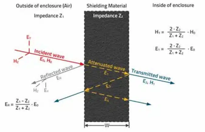
If an incident plane wave hits the barrier of the interface, reflection, absorption, and transmis-sion will occur. A part of the incident wave is reflected, a part penetrates into the material and is absorbed there, another part is partly reflected at the second transition, and parts will be reflected again (back reflection), so that finally a small part of the originally incident wave penetrates the wall. In the case of plane waves (far field), the shielding effect of an electromag-netic field through a barrier can easily be calculated. Each of the above-mentioned contributing factors to attenuation is calculated separately, and then their total contribution is summarized.