


This article based on Knowles Precision Devices blog discusses relationship of capacitors and inductors in RF circuits.
Capacitors and inductors are two closely related components that frequently work together in RF circuit design.
While both store energy, they do so in distinct ways. Capacitors store energy in an electric field and help regulate voltage changes, whereas inductors store energy in a magnetic field and resist changes in current.
Mechanical analogs help visualize their behavior:
A capacitor is like a spring.
Just as a compressed spring stores mechanical energy, a charged capacitor stores electrical energy. The relationship between force and displacement in a spring corresponds to the relationship between voltage and charge in a capacitor.
An inductor is like a mass.
Just as a mass resists changes in motion, an inductor resists changes in current. The relationship between force and acceleration in a mass system corresponds to the relationship between voltage and the rate of change of current in an inductor.
As frequency increases, capacitors and inductors exhibit opposite impedance behavior. Capacitors have lower reactance, allowing more current to pass, making them behave like short circuits. In contrast, inductors have higher reactance, resisting current flow and acting more like open circuits. While inductors still store energy in a magnetic field, their increasing impedance makes them more dominant in circuit behavior at high frequencies.
LC Circuits as the Basis of RF Resonance
When a capacitor (C) and an inductor (L) are combined, they form an LC circuit, also known as a resonant tank circuit. In such a circuit, energy oscillates back and forth between the electric field of the capacitor and the magnetic field of the inductor. This oscillation occurs at a specific resonant frequency, given by:
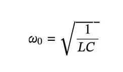
At resonance, where inductive reactance and capacitive reactance are equal in magnitude but opposite in phase, the inductor and capacitor exchange energy, creating a stable oscillation. This oscillation is essential in RF applications such as signal filtering, frequency selection, and oscillator circuits.
Thinking back to our mechanical analogies, an LC circuit is like a mass bouncing on a spring:
- The mass (inductor) resists changes in motion (current).
- The spring (capacitor) stores and releases energy (voltage variations).
- The oscillation frequency depends on the stiffness of the spring (capacitance) and the mass (inductance).
This concept is essential for designing RF filters, tuning circuits, and power stages that require precise control of AC signals, such as LLC DC-DC converters.
Maximum Power Transfer Theorem
The Maximum Power Transfer Theorem is not primarily a tool for analysis but rather a valuable aid in system design. In simple terms, the maximum power will be dissipated by a load resistance when that resistance matches the Thevenin or Norton resistance of the network supplying the power. If the load resistance is lower or higher than the Thevenin or Norton resistance of the source network, the dissipated power will be less than the maximum.
This concept is particularly relevant in radio transmitter design, where the antenna or transmission line “impedance” is matched to the final power amplifier “impedance” to achieve maximum radio frequency power output. Impedance, which represents the overall resistance to AC and DC current, is quite similar to resistance and must be equal between the source and load for the greatest amount of power to be transferred to the load. A load impedance that is too high will result in low power output, while a load impedance that is too low will not only lead to low power output but could potentially cause overheating of the amplifier due to the power dissipated in its internal (Thevenin or Norton) impedance.
Maximum Power Transfer Example
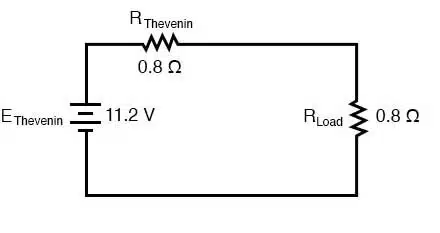
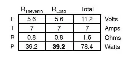
Taking our Thevenin equivalent example circuit, the Maximum Power Transfer Theorem tells us that the load resistance resulting in greatest power dissipation is equal in value to the Thevenin resistance (in this case, 0.8 Ω):
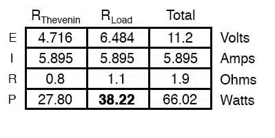
If we were to try a lower value for the load resistance (0.5 Ω instead of 0.8 Ω, for example), our power dissipated by the load resistance would decrease:
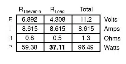
Power dissipation increased for both the Thevenin resistance and the total circuit, but it decreased for the load resistor. Likewise, if we increase the load resistance (1.1 Ω instead of 0.8 Ω, for example), power dissipation will also be less than it was at 0.8 Ω exactly:
If you were designing a circuit for maximum power dissipation at the load resistance, this theorem would be very useful. Having reduced a network down to a Thevenin voltage and resistance (or Norton current and resistance), you simply set the load resistance equal to that Thevenin or Norton equivalent (or vice versa) to ensure maximum power dissipation at the load. Practical applications of this might include radio transmitter final amplifier stage design (seeking to maximize the power delivered to the antenna or transmission line), a grid-tied inverter loading a solar array, or electric vehicle design (seeking to maximize the power delivered to drive motor).
Maximum Power Doesn’t Mean Maximum Efficiency
The Maximum Power Transfer Theorem doesn’t necessarily lead to maximum efficiency. Applying it to AC power distribution doesn’t result in optimal or even high efficiency. In contrast, achieving high efficiency is more crucial for AC power distribution, which necessitates a relatively low generator impedance compared to the load impedance.
Similar to AC power distribution, high-fidelity audio amplifiers are designed for a relatively low output impedance and a relatively high speaker load impedance. The ratio of “output impedance” to “load impedance” is known as the damping factor, typically ranging from 100 to 1000.
However, maximum power transfer doesn’t align with the objective of minimizing noise. For instance, the low-level radio frequency amplifier between the antenna and a radio receiver is often designed to minimize noise. This often requires a mismatch between the amplifier input impedance and the antenna impedance, deviating from the ideal solution based on the maximum power transfer theorem.
Impedance Matching with LC Circuits
One of the most important applications of LC circuits in RF design is impedance matching, which maximizes power transfer between circuit components. According to the Maximum Power Transfer Theorem, power transfer is optimized when the load impedance matches the source impedance.
In RF circuits, impedance matching is often accomplished using an LC matching network, such as an L-section network, which can transform a low impedance into a higher impedance or a high impedance into a lower impedance. This transformation depends on the network configuration. A series inductor and parallel capacitor increase impedance. A series capacitor and parallel inductor decrease impedance.
For example, an input matching network is critical in RF amplifier designs, where the relatively low impedance of the active gain device must match the system impedance. This ensures efficient power transfer between the amplifier and the antenna or transmission line, minimizing signal loss and reflections.
Understanding the interaction between capacitors and inductors is foundational for designing RF circuits, and this forms a solid foundation for exploring inductors in greater depth.
For more fundamentals, see the Passive Components Knowledge Blog on capacitors, inductors, filters and other EEE components.