Passive Components Blog
No Result
View All Result
  • Home
  • NewsFilter
    • All
    • Aerospace & Defence
    • Antenna
    • Applications
    • Automotive
    • Capacitors
    • Circuit Protection Devices
    • electro-mechanical news
    • Filters
    • Fuses
    • Inductors
    • Industrial
    • Integrated Passives
    • inter-connect news
    • Market & Supply Chain
    • Market Insights
    • Medical
    • Modelling and Simulation
    • New Materials & Supply
    • New Technologies
    • Non-linear Passives
    • Oscillators
    • Passive Sensors News
    • Resistors
    • RF & Microwave
    • Telecommunication
    • Weekly Digest

    Würth Elektronik Releases Heat Sinks for TO and IC packages

    Würth Elektronik ICS to Acquire MRS Electronic and Expand Vehicle Electronics Portfolio

    Indias ECMS Wave Brings New Capacity For Passive Components Manufacturing in India

    Binder Introduces Triangular Moulding for M16 and M12 Cable Connectors

    Panasonic High Precision Chip Resistors Bridge Gap Between Thin and Thick Technology

    Wk 13 Electronics Supply Chain Digest

    Samsung Introduces 35V MLCCs Flying Capacitors for USB PD Fast Charging

    New J‑STD‑075B Standard Elevates Process Sensitivity Classification for Passive and Solid-State Components

    Modelithics Expands COMPLETE+3D Library for Ansys HFSS

    Trending Tags

    • Ripple Current
    • RF
    • Leakage Current
    • Tantalum vs Ceramic
    • Snubber
    • Low ESR
    • Feedthrough
    • Derating
    • Dielectric Constant
    • New Products
    • Market Reports
  • VideoFilter
    • All
    • Antenna videos
    • Capacitor videos
    • Circuit Protection Video
    • Filter videos
    • Fuse videos
    • Inductor videos
    • Inter-Connect Video
    • Non-linear passives videos
    • Oscillator videos
    • Passive sensors videos
    • Resistor videos

    Transformer-Based Power-Line Harvester Magnetic Design

    Thermal Modeling of Magnetics

    Standard vs Planar LLC transformers Comparison for Battery Chargers

    How Modern Tools Model Magnetic Components for Power Electronics

    Advanced Loss Modeling for Planar Magnetics in the Frenetic Planar Tool

    2026 Power Magnetics Design Trends: Flyback, DAB and Planar

    Enabling Software‑Defined Vehicle Architectures: Automotive Ethernet and Zonal Smart Power

    Calculating Resistance Value of a Flyback RC Snubber 

    One‑Pulse Characterization of Nonlinear Power Inductors

    Trending Tags

    • Capacitors explained
    • Inductors explained
    • Resistors explained
    • Filters explained
    • Application Video Guidelines
    • EMC
    • New Products
    • Ripple Current
    • Simulation
    • Tantalum vs Ceramic
  • Knowledge Blog
  • DossiersNew
  • Suppliers
    • Who is Who
  • PCNS
    • PCNS 2025
    • PCNS 2023
    • PCNS 2021
    • PCNS 2019
    • PCNS 2017
  • Events
No Result
View All Result
Passive Components Blog
No Result
View All Result

Properties and Characteristics of Crystal Units

24.5.2023
Reading Time: 5 mins read
A A

This article written by Wataru Muraoka, KYOCERA-AVX Corporation explains properties and characteristics of crystal units.

Numerous devices in people‘s lives today are becoming more sophisticated. As a result, the number of crystal devices installed is increasing.

RelatedPosts

Kyocera Releases 30fs Jitter Differential Clock Oscillator

KYOCERA AVX Extends Ultra‑Broadband RF Capacitor Series

Kyocera Offers Small SAW Filters for IoT RF Modules

For example, with the evolution of autonomous driving, we are using crystal devices for many functions such as sensor systems to detect distance, camera systems to capture images, image processing systems to process captured images, and communication systems to communicate many of those digital data in and out of the vehicle at high speed.

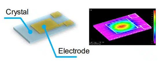
Crystal Units are a piezoelectric element which produces electricity on the surface when mechanical pressure is applied, and when electricity is applied it vibrates in a certain manner. A Crystal Unit is a product that utilizes this piezoelectric effect.

In addition, in the network market, the number of crystal devices is increasing along with the further increase in the speed of communication devices, as
well as the increase in the frequency and precision. This paper describes KYOCERA AVX’s technology for Crystal Units, one of its crystal device products.

What are Crystal Units?

Crystal Unit is a piezoelectric element which produces electricity on the surface when mechanical pressure is applied, and when electricity is applied
it vibrates in a certain manner. A Crystal Unit is a product that utilizes this piezoelectric effect.

Figure 1. shows the overall image, and Figure 2 shows the vibration mode.

Figure 1: Crystal Unit Image; Source KYOCERA AVX
Figure 2: Crystal Unit Vibration Image; Source: KYOCERA AVX

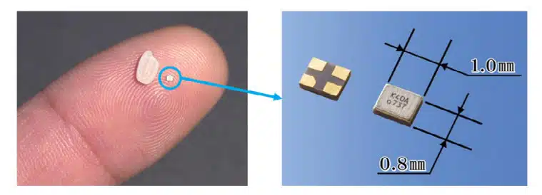
Frequency is dependent on Crystal thickness, the thinner it gets the higher the frequency. Our technology development is targeted for thinner and smaller products. Due to our own unique technology which are CVM technology and photolithography, we have realized the world’s smallest Crystal Unit in 1008 size shown in Figure 3.

Figure 3: World’s smallest Crystal Unit CX1008SB series; source: KYOCERA AVX

From here we will explain regarding increased reliability in the junction.

Figure 4: Crack for conventional crystal unit product; source: KYOCERA AVX

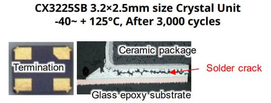
Due to the difference ceramic package and customer’s board, when the component is mounted on a board residual stress remains in the junction, which may lead to solder cracks as shown in Figure 4.

In order to improve the above, the pitch between the terminations have been shortened and termination area has been enlarged as shown in Figure 5.

Ceramic package and the glass epoxy board are electrically connected with solder. The improved junction reliability is one of the main features of this product.

Figure 5: No solder crack confirmed regarding improved product series; source: KYOCERA AVX

Miniaturization of Crystal Units

In recent years, the mounting density of electronic devices has increased due to the increasing number of functions of communication terminals for 5G communications, faster Wi-Fi®, and the electrification of onboard components.

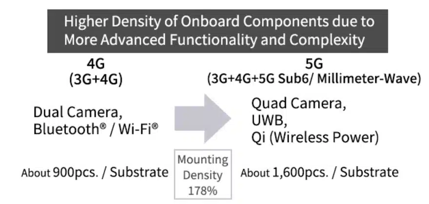
In addition, due to the limited space available in the mounting area, the size of mounted components is becoming smaller. Among them, Kyocera developed excellent photolithography and ultra-high precision machining technology jointly with Osaka University, and we have succeeded in mass producing an ultra-small crystal unit, the CX1008SB Series.

If the size is reduced from the conventional size of 1.2 x 1.0mm to 1.0 x 0.8mm, the series resistance value (CI value) will increase by about 30%. To avoid
this, it was necessary to review the circuit design of the substrate on which the crystal is mounted.

Therefore, by optimizing the design of the crystal device using Kyocera’s proprietary piezoelectric analysis technology, Kyocera achieved a size as small as 1.0 x 0.8mm while also achieving electrical characteristics equivalent to 1.2 x 1.0 mm (Kyocera’s CX1210 Series). This made it possible to use the circuit on the board without making changes.

Plasma CVM Machining

With conventional machining accuracy, when a crystal device is miniaturized there is a problem that variations in electrical characteristics become large. Kyocera has resolved this problem with its ultra-high precision machining technology which Kyocera developed in collaboration with Osaka University.

This technology is a processing method that uses neutral radicals in plasma and chemical reactions on the surface of the workpiece, enabling precise control of crystal thickness and surface conditions. This has resulted in a successful reduction in frequency fluctuation.

Plasma is radiated to crystal wafers in atmospheric pressure, triggering a chemical reaction with neutral radicals to realize equal wafer thickness.

Related

Source: KYOCERA AVX

Recent Posts

Würth Elektronik Releases Heat Sinks for TO and IC packages

31.3.2026
4

Equivalent Circuit Constants of Crystal Units Explained

26.3.2026
24

Würth Elektronik Unveils High-Current Automotive Power Inductor

24.3.2026
26

Würth Elektronik Presents Differential Pressure Sensor for HVAC and Medical

17.3.2026
21

Würth Elektronik and Grinn Launch Edge AI Cooperation

13.3.2026
24

Murata New Vibration Sensor Targets High‑Frequency Predictive Maintenance

10.3.2026
55

Kyocera Releases 30fs Jitter Differential Clock Oscillator

10.3.2026
22

Würth Elektronik IQD Awarded by EcoVadis Gold Sustainability Medal

4.3.2026
5

KYOCERA AVX Extends Ultra‑Broadband RF Capacitor Series

24.2.2026
60

Upcoming Events

Apr 21
16:00 - 17:00 CEST

Heatsink Solutions: Thermal Management in electronic devices

May 5
16:00 - 17:00 CEST

Understanding and Selecting Capacitors – Fundamentals, Technologies and Latest Trends

May 19
16:00 - 17:00 CEST

Designing Qi2 Wireless Power Systems: Practical Development and EMC Optimization

View Calendar

Popular Posts

  • Buck Converter Design and Calculation

    0 shares
    Share 0 Tweet 0
  • Boost Converter Design and Calculation

    0 shares
    Share 0 Tweet 0
  • Flyback Converter Design and Calculation

    0 shares
    Share 0 Tweet 0
  • LLC Resonant Converter Design and Calculation

    0 shares
    Share 0 Tweet 0
  • Dual Active Bridge (DAB) Topology

    0 shares
    Share 0 Tweet 0
  • MLCC and Ceramic Capacitors

    0 shares
    Share 0 Tweet 0
  • Ripple Current and its Effects on the Performance of Capacitors

    3 shares
    Share 3 Tweet 0
  • MLCC Case Sizes Standards Explained

    0 shares
    Share 0 Tweet 0
  • Capacitor Charging and Discharging

    0 shares
    Share 0 Tweet 0
  • Plastic Materials Dielectric Constant and DF

    4 shares
    Share 4 Tweet 0

Newsletter Subscription


Passive Components Blog

© EPCI - Leading Passive Components Educational and Information Site

  • Home
  • Privacy Policy
  • EPCI Membership & Advertisement
  • About

No Result
View All Result
  • Home
  • Knowledge Blog
  • PCNS

© EPCI - Leading Passive Components Educational and Information Site

This website uses cookies. By continuing to use this website you are giving consent to cookies being used. Visit our Privacy and Cookie Policy.
Go to mobile version