Passive Components Blog
No Result
View All Result
  • Home
  • NewsFilter
    • All
    • Aerospace & Defence
    • Antenna
    • Applications
    • Automotive
    • Capacitors
    • Circuit Protection Devices
    • electro-mechanical news
    • Filters
    • Fuses
    • Inductors
    • Industrial
    • Integrated Passives
    • inter-connect news
    • Market & Supply Chain
    • Market Insights
    • Medical
    • Modelling and Simulation
    • New Materials & Supply
    • New Technologies
    • Non-linear Passives
    • Oscillators
    • Passive Sensors News
    • Resistors
    • RF & Microwave
    • Telecommunication
    • Weekly Digest

    SCHURTER Introduces PPTC Resettable Overcurrent Protection for Compact Electronics

    TrendForce: CSP in‑house AI ASIC Boom Reshapes Capacitor Demand

    Würth Elektroniks Flexible EMI Shielding Sheets Provides Quick and Easy Schielding Solution

    Samsung Introduces Automotive 1206 100uF X7T MLCC for Power Rails in ADAS and SoCs

    Hirose Releases Ultra‑low Profile FPC‑to‑board Connector

    YMIN Hybrid Aluminum Capacitors for Automotive LiDAR Power Rails

    Samsung Presents Ultra‑Thin Silicon Capacitors for AI and Server PDN

    YAGEO Introduces 310VAC SMD Y2 Safety MP Capacitors for Compact EMI Filtering

    DMASS: European Components Distribution Returns To Growth In Q1 2026

    Trending Tags

    • Ripple Current
    • RF
    • Leakage Current
    • Tantalum vs Ceramic
    • Snubber
    • Low ESR
    • Feedthrough
    • Derating
    • Dielectric Constant
    • New Products
    • Market Reports
  • VideoFilter
    • All
    • Antenna videos
    • Capacitor videos
    • Circuit Protection Video
    • Filter videos
    • Fuse videos
    • Inductor videos
    • Inter-Connect Video
    • Non-linear passives videos
    • Oscillator videos
    • Passive sensors videos
    • Resistor videos

    Why Isolated DC/DC Power Supplies Fail Late, Würth Elektronik Podcast

    Designing 800 V DC EMC Filters: Calculation, Simulation and Measurement

    Current Sense Transformer Datasheet and Design‑in Guide

    Designing a USB Type‑C Flyback Planar Transformer with Frenetic’s Planar Tool

    Magnetics Design in High‑Frequency GaN Converters

    Qi2 Wireless Charging: Inductors, Capacitors and EMC Filters

    Two‑capacitor paradox explained for engineers

    Capacitances of Nonlinear MLCCs: What Datasheets Don’t Tell You

    Tapped Inductor Buck Converter Fundamentals

    Trending Tags

    • Capacitors explained
    • Inductors explained
    • Resistors explained
    • Filters explained
    • Application Video Guidelines
    • EMC
    • New Products
    • Ripple Current
    • Simulation
    • Tantalum vs Ceramic
  • Knowledge Blog
  • DossiersNew
  • Suppliers
    • Who is Who
  • PCNS
    • PCNS 2025
    • PCNS 2023
    • PCNS 2021
    • PCNS 2019
    • PCNS 2017
  • Events
No Result
View All Result
Passive Components Blog
No Result
View All Result

Engineers reinvent the inductor after two centuries

27.2.2018
Reading Time: 4 mins read
A A

source: nanotechweb news

Could the inductor be redesigned in a fundamentally new way? Yes, according to new work by researchers in the US, Japan and China who have made the first high-performance inductors from intercalated graphene that work in the 10-50 GHz range thanks to the mechanism of kinetic inductance – rather than magnetic inductance as in conventional devices.

RelatedPosts

SCHURTER Introduces PPTC Resettable Overcurrent Protection for Compact Electronics

TrendForce: CSP in‑house AI ASIC Boom Reshapes Capacitor Demand

Würth Elektroniks Flexible EMI Shielding Sheets Provides Quick and Easy Schielding Solution

The new inductors, which have both small form-factors and high inductance values, of around 1-2 nanoHenry (a combination that has been difficult to obtain so far), are a third smaller in terms of surface area than conventional devices but with the same performance. They might thus be used in ultra-compact wireless communication systems for applications in the Internet of Things (IoT), sensing and energy storage/transfer.

featured image: A spiral inductor and its simplified equivalent circuit

“The inductor was invented nearly 200 years ago, but this is the first time since then that a completely new mechanism (kinetic inductance) is being exploited (using intercalated graphene) to re-invent this fundamental passive device,” team leader Kaustav Banerjee of the University of California, Santa Barbara, tells nanotechweb.org. “This could have significant implications for wireless communications, sensing and energy storage/transfer applications for the IoT era. It also highlights a practical application for graphene beyond circuit interconnects.”

The IoT promises to connect us with as many as 50 billion objects by 2020, with a potential impact of $2.7 to 6.2 trillion per year by 2025. This revolution will require an enormous number of miniaturized, high-performance and scalable wireless connections that are driven by radio-frequency (RF) integrated circuits (RF-ICs). Another important area, that of radio-frequency identification (RF-ID), which relies on electromagnetic fields to automatically identify and track tags attached to objects, is predicted to increase to nearly $19 billion by 2026.

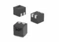
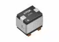
Planar on-chip metal inductors are the main types of device employed in RF-ICs and can take up as much as half of the chip area space. They are also responsible for the major part of the form factor of RF-IDs.

Scaling down difficult for on-chip inductors

However, the problem is that, unlike transistors and interconnects in IC technology that have been successfully scaled down, the same cannot be said for on-chip inductors. This is because inductors have been traditionally designed to work using magnetic fields alone, so a certain amount of inductor area is needed to capture these fields. What is more, conventional metals only have a small kinetic inductance because of their low momentum relaxation time (which is the average time for a carrier – an electron or hole – to lose its original momentum because of a scattering event).

To scale down inductors, we need to improve their inductance density. This is defined by the inductance per unit area = total inductance (Ltotal)/inductor area, where Ltotal is the sum of the magnetic inductance (LM) and the kinetic inductance (LK).

Kinetic inductance is a purely material property

Magnetic inductance is the property of an electrical conductor by which a change in current through it induces an electromotive force in both the conductor itself (self-inductance) and in any nearby conductors (mutual inductance) that opposes the change. Kinetic inductance, for its part, is the inertial mass of mobile charge carriers in alternating electric fields and so does not rely on the magnetic field.

All this means that the magnetic inductance depends on the geometrical design of the inductor itself, while the kinetic inductance is a purely material property, says Banerjee. Improving both the LM and LK should thus improve the overall inductance density, which is our goal.

Carbon nanomaterials to the rescue

Banerjee and colleagues recently found that carbon materials, including carbon nanotube bundles and multilayer graphene, are attractive materials for on-chip inductors thanks to their high magnetic inductance and high LK, which can be equal or even greater than the magnetic inductance. “We can thus use these materials to now scale down the on-chip inductor size without compromising their inductance values.”

In this work, the researchers started out with millimeter-sized multi-layer graphene sample transferred to isolating substrates that they intercalation doped with bromine.

Layer separation increases the kinetic inductance

“Intercalation involves inserting ‘guest’ molecules between the two other ‘host’ molecules in multilayered structures, which in this case are bromine and MLG respectively,” explains Banerjee. “This intercalation introduces two important properties in the MLG. First, and perhaps most crucially, it increases the separation between the adjacent graphene layers. This increase has the effect of ‘decoupling’ these layers and thereby increases the kinetic inductance by increasing the momentum relaxation time.”

Thanks to its linear electronic band structure, monolayer graphene typically has a significantly larger momentum relaxation time compared to its multi-layer counterpart. In fact, interlayer coupling in MLG transforms the linear band structure of the monolayers to hyperbolic, which leads to lower momentum relaxation times and thus lower kinetic inductance.

A new working mechanism for inductors

“Secondly, intercalation dopes the MLG and increases its electrical conductivity, which helps in improving its performance (or Q-factor).”

The work could revolutionize the way we make on chip inductors employed in analogue/RF ICs for wireless communications, and highlights a new working mechanism for these devices, he says. “Such inductors are set to become crucial in the near future where billions of connected IoT devices will send and receive huge quantities of information to each other in applications such as continuous monitoring of vital health signs and security, and also provide unprecedented connectivity for living a smarter life.”

The team, which includes researchers from the Shibaura Institute of Technology in Tokyo and Shanghai Jiao Tong University, is now busy looking into ways to further improve the efficiency of the intercalation process so that the kinetic inductance can be further increased. “This would in turn increase the inductance density and could help further downscale on-chip inductors and thus improve the area-efficiency of the chip as well as its Q-factor,” explains Banerjee. “We are also trying to make the entire inductor fabrication process compatible with back-end-of-line CMOS technology.”

Full details of the research are reported in Nature Electronics doi:10.1038/s41928-017-0010-z.

About the author
Belle Dumé is contributing editor at nanotechweb.org

Related

Recent Posts

SCHURTER Introduces PPTC Resettable Overcurrent Protection for Compact Electronics

18.6.2026
11

Samsung Presents Ultra‑Thin Silicon Capacitors for AI and Server PDN

17.6.2026
23

YAGEO Introduces 310VAC SMD Y2 Safety MP Capacitors for Compact EMI Filtering

16.6.2026
19

DMASS: European Components Distribution Returns To Growth In Q1 2026

16.6.2026
19

German Component Distribution Market Rebounds in Q1 2026 According to FBDi

16.6.2026
14

Nippon Chemi-Con Announces New Capacitor series for AI, Automotive and Immersion Cooling

16.6.2026
26

Ultrahigh Energy Storage in Lead‑Free BiFeO₃‑Based Ceramic Capacitors via Local Polar Structure Design

16.6.2026
25

Murata Expands Ansys Simulation Models for RF inductors, MLCCs, and Power Inductors

16.6.2026
26

Sumida Introduces SMD Metal Inductors for High‑Current Automotive DC/DC Converters

15.6.2026
24

Upcoming Events

Jul 14
16:00 - 17:00 CEST

EMC Design Essentials: Mastering Varistors and Common Mode Chokes

Jul 21
16:00 - 17:00 CEST

Safety by design: X and Y Interference suppression capacitors for power line filters

View Calendar

Popular Posts

  • Boost Converter Design and Calculation

    0 shares
    Share 0 Tweet 0
  • Buck Converter Design and Calculation

    0 shares
    Share 0 Tweet 0
  • LLC Resonant Converter Design and Calculation

    0 shares
    Share 0 Tweet 0
  • Flyback Converter Design and Calculation

    0 shares
    Share 0 Tweet 0
  • MLCC and Ceramic Capacitors

    0 shares
    Share 0 Tweet 0
  • Earthing Systems and IEC Classification Explained

    0 shares
    Share 0 Tweet 0
  • Dual Active Bridge (DAB) Topology

    0 shares
    Share 0 Tweet 0
  • SEPIC Converter Design and Calculation

    0 shares
    Share 0 Tweet 0
  • MLCC Case Sizes Standards Explained

    0 shares
    Share 0 Tweet 0
  • What Electronics Engineer Needs to Know About Passive Low Pass Filters

    0 shares
    Share 0 Tweet 0

Newsletter Subscription


Passive Components Blog

© EPCI - Leading Passive Components Educational and Information Site

  • Home
  • Privacy Policy
  • EPCI Membership & Advertisement
  • About

No Result
View All Result
  • Home
  • Knowledge Blog
  • Dossiers
  • PCNS

© EPCI - Leading Passive Components Educational and Information Site

This website uses cookies. By continuing to use this website you are giving consent to cookies being used. Visit our Privacy and Cookie Policy.
Go to mobile version