


This paper explains How to select the right gate resistor in terms of technology, size, peak pulse load, rated power, drift, and parasitic behaviors.
The paper was presented by Ove Hach, Vishay BCcomponents Beyschlag, Germany at the 4th PCNS 10-14th September 2023, Sønderborg, Denmark as paper No. 5.1.
Abstract
For years no week has gone by without an updated breaking news about faster and more efficient power semiconductors. Tons of papers are available discussing the power on-off behaviors to address power losses EMI and so on and so forth.
But what about the small gate resistors placed in front of the gates? This resistor controls the performance in parallel connected semiconductor layouts, avoid that transients trigger the switch by forming a low pass filter device, control the gate current spikes and avoid oscillation of the switch.
Introduction
The global energy crisis has accelerated the move towards alternative energy systems and further focused attention on energy efficiency and reducing losses in electric / electronic applications. Together these trends have hastened the adoption of new high-performance Gallium nitride (GaN) and Silicon carbide (SiC) technologies with some key advantages over traditional Silicon solutions for electronic switching. Significantly smaller physical die size, superior thermal conductivity and management, and much lower switching losses make the use of these new wide-bandgap technologies ideal for space-constrained applications that require excellent power efficiency like power supplies, drives and inverters for industrial, medical, telecom and automotive applications – Specially, in high growth demand areas like integrated Power modules used in Electric vehicles (EV) drive inverters and chargers or Satellite power converters.
Similar to many other electronic component developing technologies that involve new materials, there are trade-offs for the engineer to consider and account for in their design. Some of the most important are a function of the switching losses. For example, the resulting higher di/dt and dv / dt as well as the higher speed operation amplifies the frequency oscillation in the circuit and this very problematic noise (EMC) is a key consideration for design engineers.
Application Basics – MOSFET Gate Drive
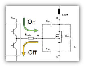
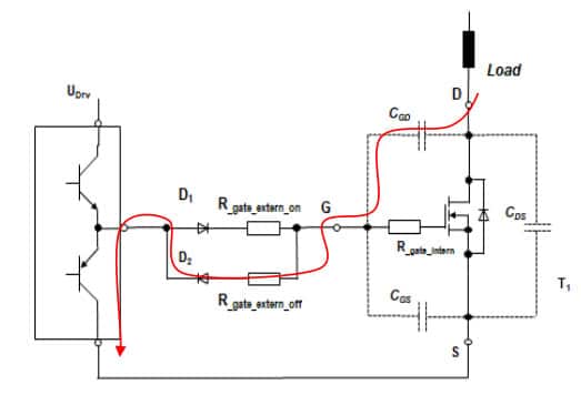
A typical circuit function uses a High-side (HS) power MOSFET and a Low-side (LS) MOSFET as switching devices to drive an inductive load. When the HS switch in ON and the LS switch OFF, the current flows from the power supply VCC to inductor Lo. When the HS switch is OFF and the LS switch is ON, the inductor current continues to flow synchronously from ground to Lo.
Electronic switches (such as MOSFETs) need to be driven in the right way from the perspective of:
- gate charge Q
- frequency of switching
- peak current capability of the driver
- fast switching, precise timing, stability of performance
The ON / OFF status is defined by the gate voltage and changes in gate voltage influence the charging and discharging of the gate loop. Switching times and associated losses depend on how fast the gate capacitor can be charged and discharged by the gate current and that gate current is influenced by the driver voltage, gate resistance and the overall intrinsic parasitics of the driver circuit.
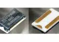
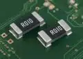
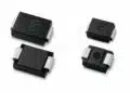
To avoid simultaneous Turn-on / Turn-off, designers typically employ a carefully selected Gate resistor solution like the high-power thick film chip, thin film MELF or IGBR high power back-contact series from Vishay that are ideal for these specific applications. This avoids the need for extended ‘dead times’ (time between HS and LS switch Turn-on) that effectively translates to power loss.
The basic considerations for selection of the Gate resistor technology series are centered around pulse power, pulse time and temperature. and stability. As a ‘rule of thumb’, where two gate resistors are employed, the On-gate resistor value should be at least double the Off-gate resistor. The Off-gate resistance value is important in avoiding parasitic Turn-on when the voltage at the drain – or in the case of IGBTs, the collector – rises.

Typical Application Characteristics
- Gate driver voltages:
- typical ON (+18 V) +15 V to +12 V
- typical OFF 0 V to -8 V
- Gate charge: 1 nC up 1300 nC
- Gate currents: mA up to “double digit” A range
- Gate rise times: several 10 ns range
- Gate frequency range: several 10 kHz up to 1 MHz
Typical Gate Resistor Characteristics
- Maximum resistance up to 100R
- High peak load
- Very short pulse duration time
- Average Power Dissipation increase with frequency
- Temperature and time change R-Value
Gate driver circuits are based on a R (resistor), C (capacitor) and L (inductor) implementation. When the resistance value is too high the losses increment. When resistance value is too low, oscillation sometimes referred to as “ringing” can occur and that is extremely undesirable in the application. The gate resistor will be required to handle a high peak load for a short duration time and the average power dissipation will increase with frequency. Functionally, it will discharge the built-up internal capacitance in the device and Miller charge. Reducing Voltage Overshoot reduces stress on the device and driver, and reducing Parasitic Inductance avoids VGS oscillation during switching.
Minimizing the length of tracks (parasitic inductance) will reduce noise in the circuit. For this reason, wire-bond or surface-mount devices are usually preferred as Gate resistors. In the case of the IGBR wire-bond series, the back contact provides superior thermal conductivity and minimizes the thermal variation between the device and the PCB. The combination of the wire-bond connection, the physical size and the sintering capability provides the designer with the ability to sinter the IGBR inside the actual high power semiconductor module or enclosure. This achieves very close proximity to the switching device, thereby reducing some parasitic elements to help with circuit noise.
Parasitic Turn-On Mitigation Checklist
- ramp up of drain voltage (IGBT: collector)
- current flow thru parasitic capacitance CCD
- current cause voltage drop over gate resistor and driver
- voltage drop needs to be smaller than threshold voltage of the switch
- optimize the value of Rgate_off to the application needs
- consider temperature and long term stabile resistors
Selection of Gate Resistor Technology
Gate resistor technology solution options range from high power thick film chip size, thin film MELF and the IGBR thin film substrate types (IGBR) that are rated up to 4 W. Other considerations in gate resistor selection include component size, precision, reliability, thermal performance between the component and the PCB, and parallel parasitic inductance. The figure below shows how application requirements transform into gate resistor technology selection.

Gate resistors are usually specified (RG) between 1 Ω and 100 Ω. Using a lower RG value will reduce dissipation across the device (EON. EOFF) but will also result in higher drive current. Due to the short rise times of wideband semiconductors, consideration must also be given to the RF ramifications of the Gate resistor and a compromise must be reached between Switching losses and EMI performance. Reducing EMI emissions can be achieved by using higher value resistors and extending the rise time of the switch, but this naturally increases switching losses.
Depending on the inductance and load in the power circuit, maximum operating voltage of the various resistor series should also be carefully reviewed as voltage spikes will occur during switching.
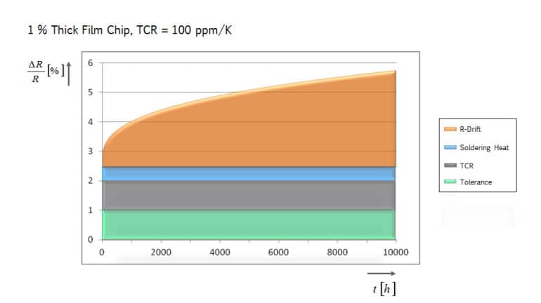
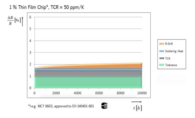
Power versus temperature & stability
Due to the high peak currents which can be in the double-digit amp range and high frequencies sometimes in the MHz range the effect of temperature on the resistor is an important consideration. Higher temperatures can cause the drift in resistance value over time. The long-term stability of the resistor value is dependent on the device construction, where products like the MELF perform exceptionally well due expanded surface of a cylinder by a factor of pi compared to rectangular surface of a single chip. Additionally, the use of stable thin film materials like NiCr also offer excellent pulse load capability. In space-constrained designs the relative location of the power switch is also important, as heat can flow from it and into the PCB. This will affect the operating temperature of the gate resistor.
Conclusions
To fully ensure efficiency advantages for wide bandgap semiconductors are realized, the optimal Gate driver circuit will need to consider the specific requirements for Gate charge Qx, the switching frequency, peak current capability of the driver, and for fast switching – the precise timing and the stability of the circuit performance.
Selecting the appropriate technology and device construction of the low ohmic value gate resistors will be crucial in achieving optimized circuit efficiency.