


Source: Deki application note and article
Important developments of IGBT’s (Insulated Gate Bipolar Transistors) over the years have been focused on increasing power handling capability and increasing reliability. Snubber capacitors have also undergone changes in construction enabling increased power handling capability. This ‘charge’ focuses on giving the reader a brief overview on the IGBT Snubber capacitor.
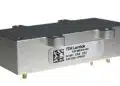
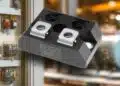
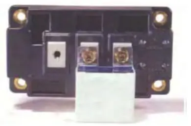
Power systems containing IGBTs must be designed so the transient voltage caused by the high dI/dt that occurs at gate turn off is minimized. Left uncontrolled, this transient voltage can exceed the blocking voltage rating of the IGBT and cause it to fail. In order to minimize the transient voltage a wound construction polypropylene film capacitor mounted as close to the IGBT terminals as possible is usually recommended. (See picture below; credit: Deki Electronics)
The acceptable amount of overshoot voltage is determined by the maximum DC voltage that an inverter power circuit is subject to and the IGBT voltage ratings. The peak current to turn off under a fault condition can be as high as 6-10 times the device current rating. This peak current under the fault condition will proportionally increase the overshoot voltage.
The switching capacity with shortest switching times which can be realized using IGBTs makes it necessary to use an extremely low-inductance circuit design. Even the low self-inductance of the power bus may induce dangerous voltage overshoots between collector and emitter which may result in the destruction of the valuable power semiconductors.
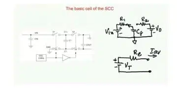
Necessity of Using the Snubber Circuit
These are placed across the various switching devices like transistors, thyristors, etc. Switching from ON to OFF state results the impedance of the device suddenly changes to the high value. But this allows a small current to flow through the switching device. This induces a large voltage across the device. If this current reduced at faster rate more is the induced voltage across the device and also if the switching device is not capable of withstanding this voltage the device may burn out. So auxiliary path is needed to prevent this high induced voltage.
Similarly, when the transition is from OFF to ON state, due to uneven distribution of the current through the area of the switch overheating will takes place and eventually it will be burned. Here also snubber is necessary to reduce the current at starting by making an alternate path.
See also article: RC snubber design for SMPS protection.
Snubbers in switching mode provides one or more of the following functions:
- Shape the load line of a bipolar switching transistor to keep it in its safe operating area.
- Reducing the transient voltages and currents during turn-ON and turn-OFF conditions.
- Removes transient energy from a switching device and dissipate the energy in a resistor to reduce junction temperature.
- Limiting the rate of change of voltage and currents during the transients.
- Reduce ringing to limit the peak voltage on a switching device and lowering their frequency.
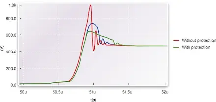
Transient voltage comparison with and without protection snubber capacitor; source: Deki Electronics
Snubber Capacitor Selection Guide:
Capacitor DC-voltage class
The maximum continuously applied DC voltage can be the rated DC voltage of the capacitor in order to ensure longer life of the capacitor. Semiconductors with 1200V blocking voltage are used with up to 900V DC-link voltage. For these applications, capacitors with a rated voltage of 1000V are recommended. For 1700V semiconductors, 1250V or 1600V capacitors are recommended, depending on the DC-link voltage. The peak voltage also has to be in the admissible values because otherwise the plastic film could be damaged. Consider also that the applied DC voltage has to be derated when the capacitor is operating at higher temperatures than the rated temperature.
Capacitance value and series inductance
The capacitance value has to be high enough to achieve sufficient voltage spike suppression during switching off. Typical values for these capacitors are from 0.1 μF to 1.0 μF. But not only is the capacitance value important for this. Also a low inductive design of the capacitor is important. The remaining inductance, caused by the loop between the terminals and the internal connections of the capacitors is responsible for a voltage spike/transient. A high capacitance value is no guarantee for a low voltage spike if the self-inductance remains. A low self-inductance can be achieved by using capacitors with wide flat terminals that can be screwed directly onto the IGBT module terminals. The capacitor should be designed so that the terminals encircle as small an area as possible and that they are directly connected to the capacitor coil without having internal wires between. Furthermore, metallized polypropylene foil capacitors should be used with plastic case according to UL94V-0.
Pulse handling capability
The inner connections of the capacitor are capable of withstanding only a limited amount of energy at each switching event. The data sheets of the supplier specify limits for pulse operation. These values can be calculated from the oscillating current or voltage waveform of the capacitor. This calculation can easily be carried out using modern digital oscilloscopes. A capacitor failure can occur only because of very high peak currents, even when the involved voltages are lower than the specified ones. In this situation the critical thing is the involved energy and normally there will be a loss of connection between metal spray and film metallization. Because of the very high energy involved the film metallization will be vaporized on the connection area to the metal spray. This will lead the capacitor to a high loss factor or even to a capacitance loss. The maximum dv/dt values are less critical because of the damped sinusoidal waveform.
RMS voltage and RMS current
A damped oscillation occurs at each switching event (on or off = twice switching frequency of the IGBT) between the snubber capacitor and the bus bar capacitance. The RMS current leads to self-heating of the capacitor. The capacitor will stabilize at a certain temperature which also depends on the ambient temperature and on the mounting conditions (e.g. temperature of power module terminals). Data sheets give values for the permissible RMS current and RMS voltage depending on the frequency. The oscillating frequency depends on the DC-link stray inductance and the snubber capacitor value. Typical values are in the range of 100 kHz to 1 MHz. The permissible RMS current decreases with the frequency because the losses increase.
Lifetime
The capacitor lifetime and failure rate is mainly affected by the operating temperature and operating voltage. The snubber circuit is formed using both R and C. Hence it is important to have the right selection of the Resistor also. It is important that R in the RC snubber, have low self-inductance. Inductance in R will increase the peak voltage and it will tend to defeat the purpose of the snubber.
Low inductance will also be desirable for R in snubber but it is not critical since the effect of a small amount of inductance is to slightly increase the recovery time of C and it will reduce the peak current in device during switching.
The normal choice of R is usually the carbon composition or metal film. Resistor dissipates the energy stored in the snubber capacitor in each transition. If we select the resistor as that the characteristic impedance, the ringing is well damped.
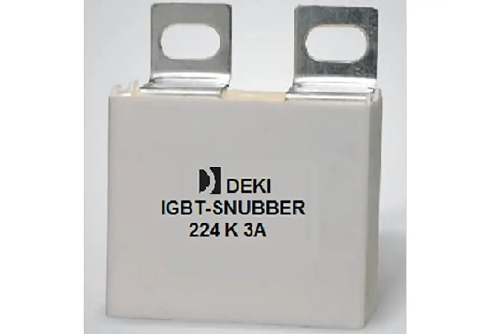
Latest Snubber Capacitors Construction and Features (Example):
IGBT Snubber Capacitor Construction:
- Dielectric: Polypropylene film
- Electrodes: Extended foil electrodes with metallised polypropylene internal series connection
- Leads: Tinned copper lugs
- Seal: Plastic case with resin sealing. Flame retardant execution (UL94V-0).
Features:
- Self-healing capability
- High-frequency
- High peak current
- High DV/DT
- High peak and RMS current capability
- Low ESR.
Applications:
IGBT snubber capacitors are used in high voltage, high current and high pulse applications such as:
- IGBT protection circuits
- snubber network
- protection circuits in SMPS, energy conversion and control in power electronics.