source: Semiconductor Engineering news
October 9th, 2017 – By: Jeff Dorsch. IPDs take the place of discretes for mobile, IoT, wearables, and are gaining traction in advanced packaging.
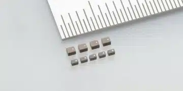
Integrated passive devices are seeing greater use within system-in-package technology and numerous applications, including the Internet of Things. The tiny devices are making their way into automotive electronics, consumer electronics, and health-care products, among other uses.
Europe is leading the way in supplying IPDs, thanks to offerings from Infineon Technologies, STMicroelectronics, and Murata Integrated Passive Solutions (formerly IPDiA). Murata Manufacturing acquired IPDiA during October of 2016, through its Murata Electronics Europe subsidiary.
Grand View Research estimates the worldwide IPD market was worth $874.6 million in 2015 and $901.5 million in 2016. IPDs used in light-emitting diode-based lighting are forecast to have a compound annual growth rate of more than 14% from now to 2025.
In addition to LED lighting, Grand View sees growth in electromagnetic susceptibility/electromagnetic interference protection IPDs, radio-frequency IPDs, and digital/mixed-signal IPDs.
MarketsandMarkets forecasts the IPD market will enjoy a compound annual growth rate of nearly 9% over the next five years, increasing from $730.1 million last year to $1.37 billion by 2022. Research and Markets is more optimistic on the growth rate, predicting a CAGR of about 17.9% in the next decade, yet it sees the worldwide market achieving lower revenue, reaching about $900.85 million by 2025.
The overall outlook for these devices is confusing. Packaging houses are seeing more widespread adoption, but not necessarily higher volumes.
ASE Technical Director Jean-Marc Yannou said IPDs are a low-volume business for Advanced Semiconductor Engineering. “We do use some IPDs and we manufacture some of them. It has grown for low-volume type of applications. They are getting quite popular for harsh-environment electronics, medical electronics, and also now for silicon photonics. It might actually increase considerably together with silicon photonics in the coming years, although it’s very hard to predict.”
One of the big advantages here is that IPDs can reduce passive component sizes by up to 70%, according to Vinayak Pandey, vice president of product technology marketing at STATS ChipPAC. “IPD technology trends show strong growth driven by the mobile and IoT markets. Thin-film IPD technology using silicon or fan-out can provide a cost-effective solution, while providing improved performance for an SiP product. Silicon-based IPDs are a cost-effective technology produced in advanced 200-millimeter manufacturing facilities, and they’re ideal for system-in-package. IPD offers a competitive advantage in size, cost, and performance.”
What is an integrated passive device?
IPDs are primarily resistors, inductors, and capacitors. They are not new, but interest in them is coming from new markets and new applications within existing markets.
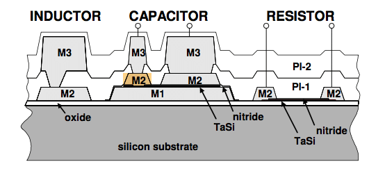
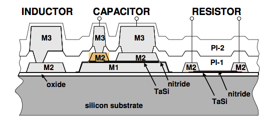
“Integrated passive devices are a collection of dedicated process technologies, allowing for integration of several passive devices on a single piece,” Pandey explained. “They generally offer high integration ratios and good performance. For thin-film IPDs, they are mainly fabricated on silicon, or glass, or other substrates that provide unique performance aid.”
Fig. 1: Thin-film IPD (illustration not to scale). Source: STATS ChipPAC
This makes them particularly attractive for system-in-package. “Drivers for system-in-package to utilize IPDs are X-Y factor, shrinkage of die, and also the Z height reduction,” Pandey said. “For performance, electrical has reduced power losses, high-frequency response, Q factor, etc. There are limitations as far as Q factor is concerned when you do thin film on silicon. Also, it’s got good reliability, and as far as system cost is concerned, there’s bill-of-materials reduction and also X-Y reduction.”
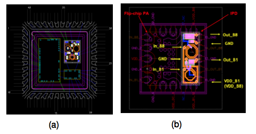
Fig. 2: (a) QFN package with three wire-bonding dies. One is IPD die. (b) QFN package with two flip-chip die, including one IPD die. Source: STATS ChipPAC
IPD manufacturing comes in two flavors—thick-film IPD and thin-film IPD technologies. “A thin-film-based integrated passive device is a silicon-based passive component integration. It’s a cost-effective way to reduce package footprint, reduce interconnection complexity, improve your performance, component tolerance, improving your yields, and improving reliability. We have applications including RF modules, ultra-wideband, WLAN, handheld devices, cellular phones..
Seung Wook (S.W.) Yoon, STATS ChipPAC’s director of product technology marketing, said IPDs are well-suited for mobile applications, the IoT, and wearable gadgets. STATS has been working with this technolgy for a dozen years. IPDs do not represent a significant portion of the company’s revenues yet, but they are expected to provide steady growth.
Some SiP customers have been able to replace 100 discrete components with two or three IPDs, according to Yoon. More typically, a single IPD can take the place of 13 or 14 discrete devices, he said.
To produce baluns and other passives, STATS ChipPAC uses a wafer fabrication process for critical-dimension control, Yoon noted. It offers a copper metallization process that deposits 8 microns or more of copper on a silicon wafer. Fabricating IPDs has typically involved a single dielectric layer of silicon nitride, but customers are looking for two or more layers on the IPDs if inductors are involved, he said. With more layers, “the cost goes up,” he observed. “Overall, cost will go down.”
The IPDs can be produced on 8-inch silicon wafers, he noted. They are typically arrayed in 2-by-2 or 3-by-3 formats. “The customer is looking for a high Q factor, quality factor,” in using IPDs, he added.
Where they fit
IPDs can be implemented in conjunction with wafer-level packaging at the chip assembly and test contractor.
“We use it for Wi-Fi connectivity and other RF applications whenever we want to design matching elevens or matching together with baluns close to the antenna with quite high precision,” said ASE’s Yannou. “We design and make RFIPs on glass, primarily, but there are other applications for high-density capacitors made from silicon. We can cite, for example, Murata Integrated Passive Solutions, which is actually constituted from the buyout of the IPDiA company.”
IPDs are found in automotive electronics and oil drilling, among other harsh environments, according to Yannou. “They can be assembled very easily in any system-in-package by using regular silicon semiconductor technologies –flip chip or wire bonding connections – in which case, you don’t have to print solder on the system-in-package substrate to place the type of capacitors or inductors,” he said.
ASE makes IPDs on 8-inch glass wafers, while some manufacturers are using 6-inch silicon substrates. “They would benefit from an interesting scaling effort, economies of scale, by moving to 8-inch or even 12-inch. Now they use the technology of deep trenches in the silicon, and they actually go quite deep into the silicon, so there might enter some warpage issues moving to larger wafers. When the need is here for very large volumes, I would think most IPD producers will move to larger-sized wafers. But it’s not needed today,” Yannou observed.
IPDs “are kind of planar,” he noted. “You can make very small components on silicon and glass. We can make planar inductors using the fine-pitch capabilities of silicon on glass. For some analog applications, IPD is not an option. And for power applications, it’s definitely not an option. Still, IPDs are probably evolving faster than discrete passives. Companies are very proactive and very smart, and will find ways to address those lower frequencies in analog and power. It might change in the future.”
Why now?
IPD technology has been around for some time. It has been a topic of discussion at conferences for more than a decade, and most companies thought the technology would progress far faster than it has.
Now the question is whether new packaging and applications will drive it from low-volume production to higher volume, where it can achieve economies of scale.
“The question is when, especially in the wireless environment,” Yannou said. “There’s always this call for miniaturization, and miniaturization is not only footprint, it’s not only X-Y axis, it’s also about thickness. And here it can make a difference. As an OSAT company, as an assemblage contractor company, ASE is interested in any form of IPDs – the ones we design and manufacture ourselves. The RFIPs on glass I told you about belong to IPD solutions from other vendors which we can integrate in our customers’ packages, especially in system-in-packages, alongside with one or several ICs.”
IPDs haven’t been widely adopted in the wireless industry yet because of their cost, Yannou said. “It’s still more expensive per active value, per nanohenry or per nanofarad, than discretes, which are such a commodity, that they almost come for free. But I believe in IPD technologies and their potential. I don’t know when it’s going to meet success in high volumes. I believe they can offer a lot in terms of reliability, low thickness, performance, performance along temperature, performance along voltage. So it’s way superior to the discrete passives we’ve been using for decades, but it’s still too expensive.”
Conclusion
Integrated passive devices are still waiting for their moment to shine in high-volume production and adoption. Right now they are competing with discrete components that carry lower price tags. That factor could change in the near future as new markets such as automotive and industrial begin picking up steam, and as advanced packaging volumes continue to grow.


