


source: EDN article
Robert L. Chao, Founder, Advanced Linear Devices, Inc. -March 12, 2016
The use of supercapacitor series stacks are growing for many systems used in backup power storage or battery life extension. One of the most critical circuit design goals for such systems is minimizing the steady state DC power dissipation. For that reason, MOSFETs deployed in circuits that balance voltage and leakage current in supercapacitor series-connected stacks of two or more, can be configured to burn zero power.
To grasp the concept of zero power burn in balancing the individual supercapacitor cells, I will describe a circuit with current burn of 0.003 micro amperes (uA), or ~0.1% of 2.80 uA. While this is not absolute zero, the amount of energy used is so minimal that it is virtually zero. Using MOSFETs to balance voltage in supercapacitor cells stacked in a series contrasts to balancing voltage using op amp, which burns quiescent current.
Supercapacitors are becoming increasingly useful in high-voltage applications as energy storage devices. When an application requires more voltage than a single 2.7-volt cell can provide, supercapacitors are stacked in series of two or more. An essential part of ensuring long operational life for these stacks is to balance each cell to prevent leakage current from causing damage to other cells through over-voltage. For those seeking more information on how this works, I invite you to read our previous submitted article, “MOSFET-based current balancing cuts power use in supercapacitor stacks”
There are actually three possible scenarios of zero power burn of balancing circuitry. First, the power dissipated can be near zero, meaning that it is substantially less than a reference power dissipation level.
In this case, l use the highest leakage current within a group of a given make and model of supercapacitor as a benchmark reference power dissipation. The highest leakage current of one of the supercapacitors used is the actual minimum leakage current possible for the entire supercapacitor stack, not including any power used by any balancing component or circuitry.
Ten percent of this reference current level can be selected as the threshold limit for zero power burn. An easy way to establish this reference current is to take the maximum leakage current specification from the supercapacitor manufacturer and use that as the reference current. A user can also establish his or her own reference current based upon the operating conditions that the system experiences, including, for example, temperature or aging effects. All supercapacitors deployed in a system should first be independently tested for this reference leakage current.
The second scenario is that the possible power dissipation is actually zero at a steady state DC level.
The third scenario is that the power dissipation of the balancing circuit dissipates negative current burn of the supercapacitor stack, meaning that after the balancing circuits are installed, the total power burn is less than when there is no balancing circuitry. This is possible because MOSFETs operate by changing the balancing voltage bias of each of the supercapacitor in a series stack so that the highest leakage of the same benchmark supercapacitor is actually reduced by reducing its voltage bias after balancing is achieved. For any given supercapacitor, a reduced voltage bias reduces its leakage current level as well.
To understand how these three scenarios play out and achieve zero power burn, it is best to go through an example and analyze in three small steps what actually happens when a SAB MOSFET goes through its balancing act.
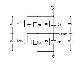
Supercapacitors connected in series with MOSFET auto-balancing

FIGURE 1: Two supercapacitors stacked in series with MOSFETs.
The above Figure 1 shows a pair of SAB MOSFETs placed across two supercapacitors. SAB MOSFET 1, or M1, is connected across C1, so input VIN1 of the SAB MOSFET is equal to supercapacitor voltage VC1. M2 is across C2 so VIN2 is equal to VC2.
There is leakage (bias controlled) current going through each one of the MOSFETs, referred to as lOUT1 for M1 and IOUT2 for M2.
Notice the equation, which states: V+ = VIN1 + VIN2 = VC1 + VC2. In other words, the two voltages across M1 and M2 are equal to the two voltages across both supercapacitors C1 and C2.
The total leakage current now becomes equal to IC1 + IOUT1 = IC2 + IOUT2.
A step-by-step example will illustrates how Supercap Auto Balancing (SAB) MOSFETs balance supercapacitor stacks with zero power burn. Assume that supercapacitors C1 and C2 have same capacitance values but different leakage currents profiles as shown in the graph featured in Figure 2 below.
An ALD910024 SAB MOSFET device is used for this example to highlight the tremendous swings in current levels. Cells C1 and C2 leakage current characteristics as a function of cell voltages were shown in the graph. With no balancing, leakage currents of C1 would follow its curve whereas that of C2 would have followed the dotted line to reach a balanced leakage current level of 1.1 uA for both cells, reaching VC2 = 2.9V, exceeding its rated voltage. Adding SAB MOSFETs would bend C2 leakage current curve to follow IC2 + IOUT2 curve instead. The leakage currents of C1 and C2 would now balance at 2.203 uA, at VC1 = 2.15V and VC2 = 2.45V respectively, protecting both cells from over-voltage.
MOSFET active balancing while achieving zero power burn

Figure 2: Adding ALD ALD910024 SAB MOSFETs would bend C2 leakage current curve to follow IC2 + IOUT2 curve.
MOSFETs interact with supercapacitors for zero power burn

The circuit action in Figures 2 and 3 above can best be illustrated in three separate smaller steps.
At Step 1, initially when VOUT voltage is at 2.30V, the leakage currents of IOUT1 + IC1 add up to 2.9 uA while IOUT2 + IC2 add up to 0.9 uA. In other words, the leakage currents are not in balance while VC1 = VC2 = 2.30V. Therefore VOUT = 2.30V voltage is going to rise a little bit as IC1 current charges C2 up until SAB MOSFET M2 is turned on a little bit harder while M1 is turned off a little bit softer.
As SAB MOSFET output current changes exponentially with its bias voltage, IOUT1 and IOUT2 changes exponentially in opposite directions with small VOUT voltage changes.
At Step 2, which is an arbitrary intermediate voltage point, VOUT voltage now rises to 2.40V, which translates to VC1 = 2.20V and VC2 = 2.40V. The total leakage current equation is still IC1 + IOUT1 = IC2 + IOUT2.
Now let’s take a look at the different currents under this new voltage condition. IC1 is now approximately 2.40 uA (see graph in Figure 2). IOUT1 is now at approximately 0.01 uA (see datasheet of ALD910024). Similarly, IC2 is at approximately 0.85 uA and IOUT2 is at approximately 1.0 uA. The leakage currents of IOUT1 + IC1 now add up to 2.41 uA while IC2 + IOUT2 add up to 1.85 uA. The leakage currents are still not in balance, which forces VOUT voltage to continue to rise.
Without the SAB MOSFETs, VOUT voltage continues to rise towards 4.60V. If it does, it will slowly destroy C2 as the VC2 = VOUT voltage exceeds 2.7V maximum rated voltage towards 2.9V, causing for example, an open circuit to C2 and rendering the entire supercapacitor series stack to become inoperative in a catastrophic failure event.
At Step 3, the VOUT voltage reaches 2.45V. At this VOUT voltage, all the currents are again changed. VC1 = 2.15V and VC2 = 2.45V. IC1 is now approximately 2.20 uA (see graph in Figure 2). IOUT1 is now at approximately 0.003 uA. IC2 is at approximately 0.90 uA and IOUT2 is at approximately 1.303 uA. The leakage currents of IOUT1 + IC1 now add up to 2.203 uA while IOUT2 + IC2 also add up to 2.203 uA. The leakage currents are now in balance, which stabilizes VOUT voltage at about 2.45V. VC1 and VC2 voltages are both within the 2.70V maximum rated voltage limits, and without any further changes, will not damage either of the two supercapacitors C1 and C2.
Any attempt to increase VOUT voltage will meet with significant increases of IOUT2 thereby limiting further VOUT voltage increase. At this point VOUT resists any further changes due to minor changes in supercapacitor leakage currents of both C1 and C2. When this equilibrium point is reached, the total leakage current of IOUT1 + IC1 is now ~2.203 uA instead of the IC1 of 2.80 uA without leakage current balancing. This example illustrates that “negative”, or below zero power burn is possible when the balancing circuitry utilizing SAB MOSFET is deployed.
In this example, the extra power is dissipated by IOUT1 which is about 0.003 uA. IC1 of C1, now at ~2.20 uA is the dominant leakage component internal to the supercapacitor, and it is less than the reference leakage current specified as 2.80 uA at 2.3V cell voltage. Net additional current burn is 0.003 uA, ~0.1% of 2.80 uA, which is approximated to zero power burn. Note that this 0.1% is that of the leakage current specification of the supercapacitor. So if that leakage current is greater or lesser, for different make or models, the extra power burn can be scaled accordingly.
For circuits described above, MOSFETs sense that the voltage wants to go up, so one of them starts leaking current very quickly, without allowing the voltage to go up much. Because it is exponential in nature and the current goes up, it will automatically float to a point where the MOSFET current IOUT1, plus the IC1 current would be equal to the leakage current of MOSFET, IOUT2 plus IC2.
There is a push-pull dynamic relationship. In other words, there are two supercapacitors and two MOSFETS, but only one MOSFET is turned on harder at any given time while the other MOSFET would be turned on a little softer. Since there is no way to know which supercapacitor has higher leakage, placing the MOSFET across both supercapacitors will balance the network automatically. Since the specific leakage of each cell is unknown, the one that has the higher leakage would be automatically balanced by the corresponding MOSFET. When a MOSFET is placed across each supercapacitor, it automatically balances the system, by equalizing whichever supercapacitor has the highest leakage current.
To summarize, MOSFETs can:
- lower additional leakage current to zero levels completely and automatically balance supercapacitors
- offers low component count and low implementation costs
- provide simple and yet elegant solution
- offer scalability to any number of supercapacitors
- adjusts for changing environmental conditions and leakage currents.
The examples illustrated above explain the zero power dissipation operation of the balancing circuit action. However, there are numerous other possible combinations, where the SAB MOSFET balancing solution, while adding little or no leakage, does allow a lower voltage bias on the leakier supercapacitor. The actual total leakage current, and hence the power dissipation caused by the series-connected supercapacitors can be potentially less than not balancing the circuit at all.
Selecting the right SAB MOSFET requires knowledge of the supercapacitor operating voltage and maximum rated leakage current. This balancing method limits leakage current better than any other method. SAB MOSFETs also actively adjust to different temperature or supercapacitor chemistry changes. A designer can just pick the maximum operating voltage margin and the maximum leakage current for the particular supercapacitor(s) and look up the correct SAB MOSFET part number. For more information, go to the ALD website and search: sab mosfet.