


This paper on current sense chip resistors was presented by Stephen Oxley, TT Electronics at the 3rd PCNS 7-10th September 2021, Milano, Italy as paper No.3.1. and voted by attendees as:
OUTSTANDING PAPER AWARD
The most cost effective and simplest way of converting a measured current to a voltage signal is to use a low ohmic value current sense resistor. The increase in products containing batteries, motors or actuators which call for current monitoring or control has led to huge growth in the market for current sense chip resistors with values below one ohm over the last two decades. But more recently, driven by power efficiency demands and enabled by low noise sense voltage amplifiers, the value range has been extended downwards from milliohms to hundreds of micro-ohms.
Such low ohmic values present challenges to the user at many stages in their design and manufacturing processes. This paper considers the nature of these challenges and suggests strategies to overcome them. The stages considered are component selection, PCB layout design, verification of the ohmic value of unmounted components, critical assembly processes, and expected ohmic values during product life. At each stage there are potential pitfalls but also opportunities to quantify and minimise error and variation.
Although sub-milliohm chip resistors are still just chip resistors, it is advisable to treat them as being a separate class of component, and to discover the particular considerations and techniques that enable their successful use.
COMPONENT SELECTION
COMPONENT SELECTION
Termination Styles
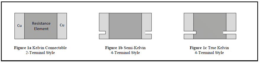
It is well known that to restrict the temperature sensitivity of a resistor-based current sensing circuit it is essential to restrict the total terminal resistance from copper which is common to both the current carrying circuit and the voltage sense circuit. This is because this element of the total measured resistance has a temperature coefficient of resistance (TCR) of +3900ppm/°C and this contributes to the total TCR in proportion to the resistance ratio. For example, a total terminal resistance of 100µΩ, that is 50µΩ at each end, for a 1mΩ resistor contributes 100µΩ/1000µΩ x 3900ppm/°C = 390ppm/°C to the TCR. This contrasts with the TCR of the resistance element itself which is typically better than ±30ppm/°C. This separation between the current carrying and voltage sense circuits is referred to as a Kelvin connection, and clearly this issue becomes more important as the nominal ohmic value is reduced.
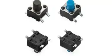
There is a spectrum of termination styles to address this problem. The commonest is the Kelvin connectable 2-terminal resistor of Figure 1a. Whilst this is often the lowest cost route it does place the onus on the PCB designer to realise a Kelvin connection in the PCB track layout, and we shall look in detail later at how this may best be achieved. Such a component must have a low termination resistance since the Kelvin connection strategy necessarily ends at the surface of the termination. Figure 1b shows an intermediate component type where four solder terminals are provided, but the separation of circuits does not extend all the way into the resistor element. Figure 1c shows a true Kelvin format where there is no current carrying termination at all within the voltage sense circuit. The latter two types offer error-proof PCB layout design and the lowest achievable magnitude of TCR but generally at a higher cost.
Element Materials
Low value resistors can be made from both thick- and thin-film materials, but the lowest values available in these technologies are in the multiple milliohm range. Both types are relatively susceptible to damage from high current surges and, in the case of thick-film technology, the lowest values are associated with high TCR values of several hundred ppm/°C and so are suited only to low precision use.
For these reasons most current sense chip resistors are based on a bulk metal element. This may be either a foil supported on a substrate or a self-supporting metal element. Whilst the former option allows to use of thin metal layers to achieve higher values, the latter lends itself to sub-milliohm values.
There is a range of alloys of differing resistivities which are selected by device designers to provide the required ohmic value within the dimensional constraints of the product. From the point of view of the user the material choice is often unimportant, but there are two exceptions. One is the control of thermally generated errors and the other is application for non-DC circuits.
A copper terminated metal element chip resistor contains at least two boundaries between dissimilar metals. These act as thermocouples and generate a thermoelectric voltage in the presence of a temperature gradient. Furthermore, they are connected in series, and, because of the symmetry of the component, are of opposite polarity when the resistor element itself is the main heat source. As a result of this, if the temperature distribution across the chip resistor is symmetrical, any generated thermoelectric voltages will be cancelled out.
Figure 2a illustrates this balanced state in which the thermal voltages V1 and V2 are equal. Figures 2b and 2c show an example of imbalance due to the external influence of a heat source and a heat sink, respectively. This would lead to a finite value of V1 – V2 which would sum with the measured sense voltage and create a source of error.
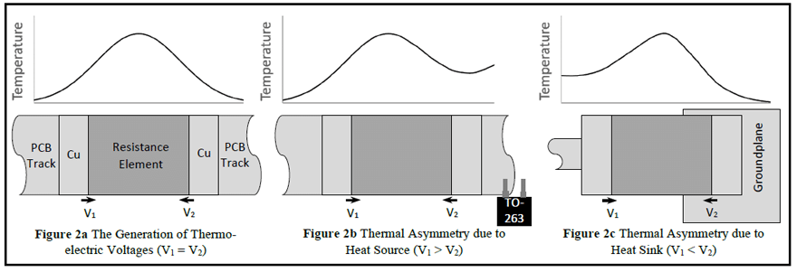
In many designs it is simply not possible to guarantee thermal symmetry under all operating conditions, and in such a case a part which employs a resistance alloy with a low thermoelectric voltage against copper should be chosen. Such alloys contain manganese in a copper nickel alloy in which the proportion of copper exceeds 80%. The thermoelectric voltages generated across a junction with copper can be as low as 3µV/°C, which is an order of magnitude lower than for a copper nickel alloy.
The second application-specific driver for resistance alloy selection is the need to avoid iron-bearing alloys in circuits where AC or rapid step changes in DC need to be tracked accurately, as this is not possible with ferromagnetic alloys.
Thermal Design Format
A problem inherent in the use of resistive current sensing is the generation of heat at a rate proportional to the square of the current. This may need to be restricted for one of two reasons. Firstly, we have the need to reduce the effect of temperature increase on the linearity of the component which can stem from TCR or from thermoelectric voltage errors. Secondly, it is necessary to avoid overheating the resistance alloy which can lead to irreversible ohmic value change.
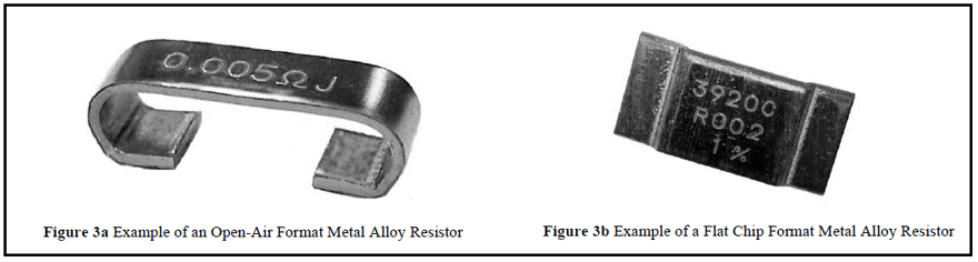
This consideration calls for careful thermal design of the assembly and begins at the component selection stage in response to the basic decision as to where the heat generated is to be dissipated, whether in the air or in the copper PCB tracks. The answer to this will depend upon the overall thermal management strategy. A well-ventilated assembly with either a high thermal loading already on the PCB, or with temperature sensitive components, would benefit from a resistor which dissipates heat into the air. On the other hand, a PCB which is heatsinked, or has no excess of heat generation and no temperature sensitive parts, can employ a resistor which dissipates heat mainly to the PCB tracks.
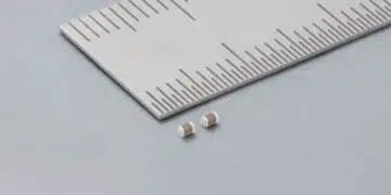
An example of a primarily air dissipating open-air format is shown in Figure 3a. This can sustain a temperature rise of the hotspot above the solder joints well in excess of 100°C and its flexible nature makes it virtually immune to temperature cycling or board flex stresses on the solder joints. An example of the primarily PCB dissipating flat chip format is shown in Figure 3b. This benefits from low profile and is generally the lower cost option.
Commonest Type
Having considered the many options of termination style, element material and thermal design format, the commonest type of sub-milliohm resistor is a 2-terminal metal element chip resistor, and this is the type which will be considered hereafter.
PCB LAYOUT DESIGN
PCB LAYOUT DESIGN
Near-Kelvin Connection
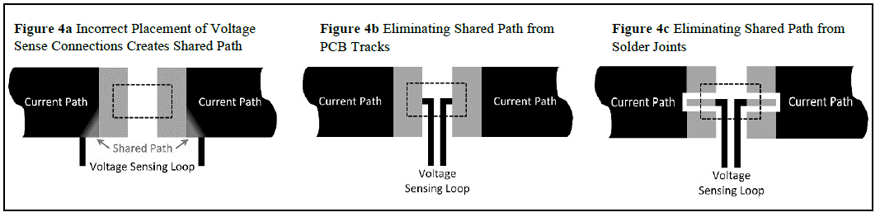
The PCB layout design around a very low value resistor is critical to its performance and the most important aspect of this is the fact that four rather than two tracks must be provided to form a Kelvin connection, even where the component itself has only two terminals. The aim is to minimize the conductive path shared between the current path and the voltage sensing loop (Figure 4a), which would increase both the effective ohmic value and the TCR of the mounted part. This may be achieved by connecting the voltage sense tracks to the inner edges of the solder pads (Figure 4b.) One can also take this a step further and split the voltage sense pads from the current path pads, so that the solder joints themselves are also removed from the shared path (Figure 4c.) By this method it is possible to approach the accuracy obtained from a true four terminal resistor.
Furthermore, a study [1] by Analogue Devices based on TT Electronics’ ULR3 0.5mΩ mounting pad options has shown that a mounted value tolerance close to 1% may be achieved on a 1% tolerance component, indicating low additional error due to mounting effects, by using a centralised, isolated sense pad design similar to that of Figure 4c.
Minimisation of Sense Loop Area
A source of error where high currents which are AC or changing DC are involved is due to the voltage sensing loop linking with changing magnetic fields. This can induce a noise signal superimposed on the desired voltage sense signal. In order to reduce this, the loop area contained within the sense resistor, the two voltage sense tracks and the sense circuit input should be minimised. This means keeping the sense circuitry as close as possible to the sense resistor and running the voltage sense tracks close to each other. A good way to keep these tracks really close is to superimpose them in different PCB layers. Where long track runs are unavoidable, it is also possible to use periodic vias to cross over the tracks into alternate layers. This replicates on a PCB the effect of a twisted pair cable, which, by means of cancellation of induced voltages, allows the circuit to withstand the effect of any changing magnetic fields which have small variation across the spatial periodicity of the twisting.
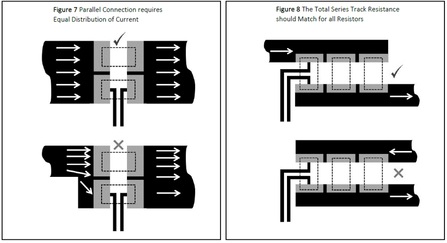
Connecting Multiple Resistors in Parallel
Designers are sometimes forced to use more than one current sense resistor connected in parallel, either to meet a high power or surge rating, or to achieve an ohmic value lower than the minimum available. This is problematic but possible. Resistors may be connected in parallel with voltage sense connections made to just one of the resistors, provided the track layout ensures equal distribution of current between all of the resistors. For example (Figure 7), the position in the current trace in which the resistors are placed should be well clear of bends or constrictions which could affect the distribution of current density. The goal is to ensure that the total track resistance in series with each resistor should be the same (Figure 8), so that the sensed resistor carries the required fraction of the total current. Moreover, this ensures that the proportion of the total current carried by the sensed resistor does not vary with temperature, as would otherwise happen with unequal series track resistances as a result of the high TCR of the copper PCB tracks.
Design for Heatsinking
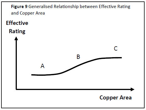
A flat chip resistor dissipates over 80% of its heat by conduction into PCB tracks, and so providing sufficient copper area to act as a heatsink is important. Copper area is for this purpose defined as the total area directly surrounding the solder pads including the first two squares of connected tracks. The general relationship between effective power rating and PCB copper area is as indicated in Figure 9. This can be divided into three distinct regions.
In region (A) there is relatively low thermal conduction through copper connected to the pads and conduction by substrate and convection to air predominate. In region (B) the copper connected to the pads acts as a heatsink to raise the effective power rating. In region (C) further increase in copper area gives diminishing returns as the internal thermal impedance of the chip restricts the rating.
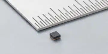
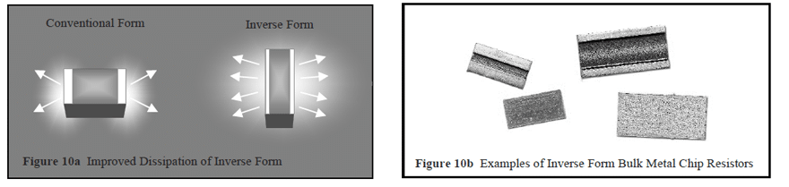
This limiting factor of the internal thermal impedance may be lowered significantly by changing the orientation of the resistor. If the terminations are formed on the longer edges of the chip rather than the shorter edges, the solder joint width is approximately doubled and the maximum distance from film centre to termination is approximately halved. The principle is illustrated in Figure 10a. TT Electronics’ ULR2N and ULR3N, shown in Figure 10b are examples of products which make use of this enhanced cooling method.
The resistor datasheet should contain information on the mounting conditions used to obtain the rated power and this indicates the minimum copper area which a designer should provide.
MEASUREMENT
VERIFICATION OF THE OHMIC VALUE OF UNMOUNTED RESISTORS
The task of measuring the ohmic value of resistors during the process of received material inspection or pre-placement verification is normally trivially simple. However, sub-milliohm resistors are far more difficult to verify and generally require custom fixturing and a specialist measurement system. Verification by a pick and place system must generally be limited to checking that the ohmic value is below a certain measurement threshold.
Fixture Requirements
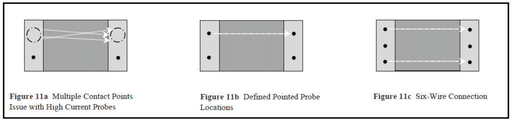
It is clear that a four-wire Kelvin connection must be made to the terminations of the resistor, but it is also essential to select the correct type of probe, the correct contact locations, and the correct connection format.
As measurement currents in the region of 5 to 10A are commonly used, it would seem to be appropriate to use a high current sprung probe for the current connections. However, such probes tend to achieve their low contact resistance by having multiple contact points to the termination surface, typically in a circular ring or star shape. Figure 11a illustrates how such a probe has unpredictable and variable contact locations which can vary with each application of the probes giving rise to small but significant variations in the direction of current flow through the component. This in turn leads to variations in the measured ohmic value. For this reason, it is advisable to use single sharp point probes for the current as well as for the sense contacts, as this will set up a precisely defined current flow through the component, and repeatable ohmic value measurements (Figure 11b). If the current requirements are simply too high to allow the use of single sharp point probes, then two probes may be employed for each current connection. This six-wire arrangement (Figure 11c) has the additional benefit of setting up a symmetrical current flow pattern closer to that seen in operation on a PCB.
The standard contact X and Y spacings for the probe tips should be stated on the datasheet or otherwise advised by the manufacturer. The probe contact pattern should be centred in both directions on the component, as both lateral and longitudinal eccentricity will affect current flow patterns and hence the ohmic value readings. Actual contact point positions may best be verified by measuring the locations of indentations in the terminations of a measured component. The fixturing created to ensure accurate contact locations on the component will require maintenance to replace worn probe tips and to ensure no misalignment arises. A repeatability & reproducibility study should be performed to ensure that measurement variation with repeated use and alternative users is acceptable.
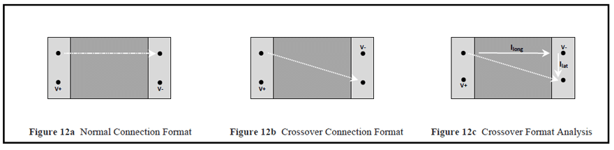
The connection format should also be specified and is usually with current contacts on one side of the chip and voltage sense contacts on the other, as in Figure 12a. A crossover format as in Figure 12b may also be used and, for a given set of location point spacings, this will result in a lower ohmic value reading. This is clear when we consider how the diagonal current flow path may be resolved into a longitudinal and a lateral component (Figure 12c.) The longitudinal component is associated with most of the voltage drop and this is picked up by the sense terminals with the expected polarity. But the lateral component which gives rise to a smaller voltage drop is picked up by the sense terminals with inverted polarity, and therefore reduces the measured value.
Measurement System
The measurement system itself needs to be capable of measuring ohmic values in the 100µΩ to 1mΩ range with a level of uncertainty which is small compared to the component tolerance. This may be achieved with a specialist micro-ohmmeter or with separate programmable current source and millivolt meter. A typical current of 5A in a 200µΩ ±1% component under test will give rise to a sense voltage of 1mV and the combined uncertainty of the current setting and the voltage measurement should be below 0.1%. The current setting uncertainty can generally be kept very low, and if necessary mitigated by independently measuring the actual current with a high accuracy ammeter. This means that the voltage measurement uncertainty would need to be 0.1% of 1mV, which is 1µV.
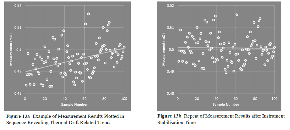
In order to mitigate thermal drift errors, it is advisable to leave the measurement system for at least an hour between switch on and use. Figure 13a shows measurement data obtained from a sample of resistors which indicates an upward trend in mean ohmic value which could not be accounted for by any process changes in their manufacture. Figure 13b shows the repeat measurement results made after an appropriate stabilisation period.
Some thermal drift may also be seen within the individual measure cycle due to component heating. Whilst the power dissipated in the element may be quite low, the point contacts can have relatively high resistance and thus generate heat which may affect the result. For this reason, the time interval between applying the current and measuring the voltage should be minimised and, if possible, standardised.
Two other methods are commonly employed to minimise the effect of error sources in such measurements. The first is the use of averaging of multiple readings taken over a time period which is an integer number of power line cycles, and this aims to achieve temporal cancellation of induced power line noise. The second is reversal of polarity during the measurement cycle which aims to detect and correct for any imbalanced thermoelectric voltages. Dedicated micro-ohmmeters often have such functions built in, but a system made from separate source and measure equipment may require programming to achieve the same result.
Product-Specific Offsets
The ohmic value measured in the manor specified by the manufacturer and taking into account all of the above-mentioned factors may still be different from the value obtained when the part is mounted on the recommended pad layout. This is the case for two reasons. Firstly, the current flow through the resistor will not be the same when using one or two point contacts at each terminal as when using a solder joint which, if voiding is low, connects to substantially the whole of the lower termination surface. Secondly, the voltage sense separation normally needs to be somewhat greater than the minimum theoretically possible, in order to allow for tolerance in the location of probes relative to the resistor. For a mounted part by contrast, the voltage sense solder joints should always connect to the innermost points of the termination surfaces.
For these reasons it is common practice for manufacturers to have two standard methods for measuring ohmic values of sub-milliohm resistors. The first is to mount the part onto a defined Kelvin connected test PCB, and this is the definitive way to establish ohmic value. The second is to use probed connections, as described previously, and to determine a standard mounting offset, normally negative, which is summed with the probe measured value to indicate the predicted mounted value:
Mounting offset = mounted value – probed value
This offset will vary depending on the termination dimensions, which in turn can be a function of the nominal ohmic value, and so it should be regarded as product specific.
Clearly aligning the results of these two methods so as to reduce the magnitude of the product-specific offset to zero would be useful, as it would enable a user to verify product value without needing to engage in detailed technical discussions with the manufacturer. There may be scope for achieving this by using the crossover format of connection (Figure 12b) and adjusting the lateral spacing so that the reduction in measured value cancels the increase in measured value which is the result of increasing the longitudinal spacing above the absolute minimum. Further work will need to be done to establish whether this is a practical possibility.
ASSEMBLY
CRITICAL ASSEMBLY PROCESSES
The assembly processes which are critical to achieving low mounting-related errors in ohmic value are solder paste printing, component placement and reflow.
Solder Paste Printing
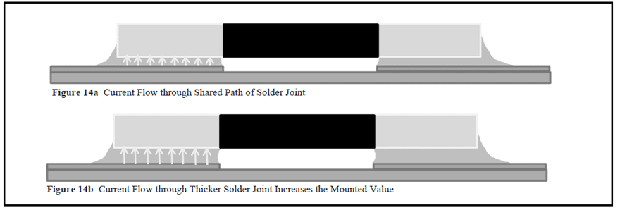
The thickness of solder in the finished solder joint has a direct bearing on the mounted ohmic value. This is because the vertically resolved component of current flow through the solder joint, as shown in Figure 14a, is in a shared path with the voltage sense loop which connects at the upper surface of the copper PCB pad. It therefore follows that increased solder thickness, as shown in Figure 14b, will result in an increase mounted value.
The magnitude of this sensitivity may be estimated as follows, for a typical case.
ΔR/ΔL = 2ρ/A
Where
- ΔR is incremental increase in mounting offset (mounted measured value – probe measured value) (Ω)
- ΔL is incremental increase in solder thickness (m)
- ρ is the resistivity of the solder (Ωm)
- A is cross sectional area of the solder joint in the horizontal plane (m2)
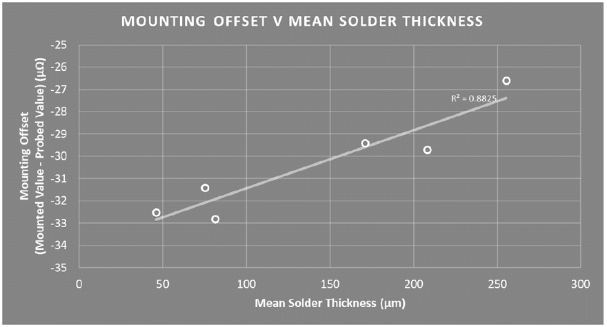
For TT Electronics’ LRMAP2512-R0005FT4, 500µΩ ±1% in a 2512 footprint, the value of A is approximately 8.32mm2. For SAC305 alloy solder the value of ρ is 1.4 x 10⁻⁷ Ωm. The factor of 2 reflects the fact that there are two terminations.
This yields a sensitivity ΔR/ΔL = 33.7µΩ/mm.
A typical stencil thickness is 130µm, and this thickness of solder would be predicted to result in a mounted value increase of 4.4µΩ which is about 0.9% of the nominal value. Variations in solder thickness of around ±20% around this value would then result in mounted value changes of nearly ±0.2%. This is one reason why it is not realistic to expect a ±1% tolerance on mounted values from a ±1% tolerance resistor.
Figure 15 shows the results of a study looking at this sensitivity in the case of the example component referenced above. It yields a result of 28µΩ/mm which agrees broadly with the theoretical prediction. The fact that the empirical sensitivity is lower may be due to the fact that conduction through the solder fillet has been ignored, and accounting for this would involve increasing the effective area A.
The same analysis may be applied to other components by substituting the underside termination areas (A) relating to them. It is worth observing that large area and long-side terminations which are often provided for reasons of thermal management to improve the thermal contact to PCB tracks also have the benefit of lowering the sensitivity to variations in solder thickness.
Component Placement
The component placement positional accuracy of current pick & place systems based on aluminium platforms is in the range 50 to 100µm, reaching down to 20µm for steel platforms [2]. Once the trade-off between accuracy and speed is applied, chip components are commonly placed with around 80µm accuracy. This is perfectly adequate for normal resistors where mounting pad sizes are designed to accommodate this degree of variation.
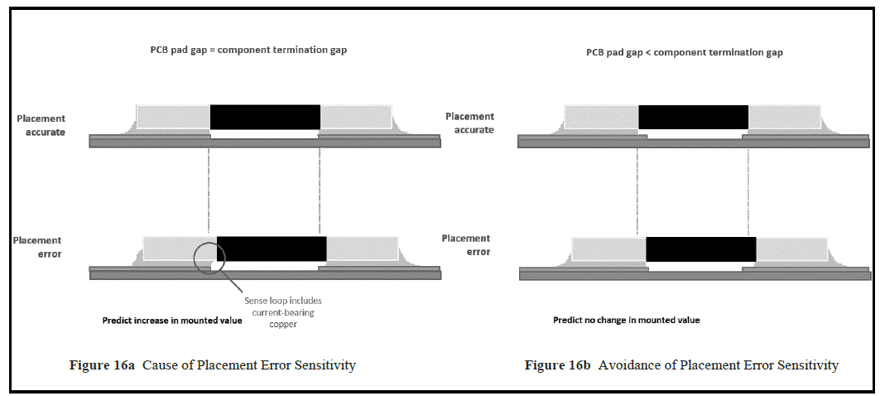
However, for sub-milliohm chip resistors care should be taken to avoid an overhang of the termination on the interior edge of a mounting pad, beneath the component. This has the effect of bringing some current carrying termination inside the voltage sense loop, thereby raising the mounted value as shown in Figure 16a. This would apply where the gap between the mounting pads exactly equals the gap between the terminations. This potential problem may be overcome by making the gap between mounting pads smaller than that between the terminations by an amount commensurate with the magnitude of the placement accuracy. Figure 16b shows how the same degree of longitudinal placement error has no effect on mounted value when this has been done.
A practical study performed on TT Electronics’ LRMAP2512-R0005FT4 mounted on its recommended solder pads gave the results shown in Figure 17 indicating no correlation between mounting offset and longitudinal placement error up to about 100µm. This indicated no correlation and therefore no indication of placement error sensitivity.
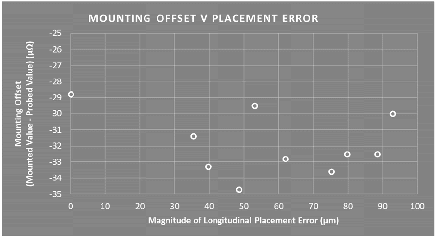
A similar study on the effect of orientation angle errors also showed no sensitivity within the range ±2°. Transverse placement accuracy is not expected to cause issues provided the pad width is sufficient, and so has not been studied.
Reflow
The exposure to heat during the process of reflow can permanently affect the value of a resistor by altering the element material’s resistivity and this is normally established by initial testing by probed measurement and final testing by mounted measurement after reflow, to establish the value shift. However, with sub-milliohm resistors this is clearly problematic since, as we have seen, a number of factors can complicate the comparison in value between mounted and unmounted parts. The Resistance to Solder Heat test (e.g. 260°C ±5°C for 20s ±1s) for such resistors therefore tends to reflect the total value change due to a range of factors beyond the effect of heat exposure on the resistivity of the resistance element material.
If one wishes to study the effect of reflow on the element resistivity there are a number of approaches that may be used. The first is to de-solder mounted parts and measure the final value in the same probe fixture as used for the initial value measurements. Drawbacks of this approach are the presence of excess solder affecting the termination resistances and the fact that additional, uncalibrated heat exposure occurs during de-soldering. An alternative is to probe on the upper surface of the resistor terminations both before and after re-flow. This may not give the correct resistance value, depending on the degree of symmetry the resistor has about the horizontal plane, but for resistance change measurements that does not matter. However, the presence of the PCB tracks can still affect the resistance of the terminations. Possibly the best method is to perform a “dry” reflow whereby the components are simply sent through a reflow process in a heat-proof container. Since the test conditions before and after are now identical, any resistance changes which are statistically significant, allowing for the repeatability of the probe measurement, may be ascribed to alloy resistivity shift.
A practical issue that can arise when reflowing components with larger termination areas is that of voiding within solder joints. If this is severe it will have the effect of reducing the cross-sectional area of the joint and therefore increasing sensitivity to variations in solder thickness. Furthermore, there is the possibility of voids having a greater effect on mounted value if they occur in the vicinity of the voltage sense connection, as illustrated in Figure 18a.
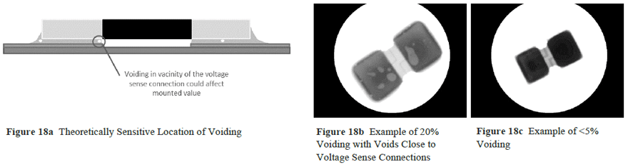
Figure 18b shows an X-ray of one of the mounted parts used in this study which gave rise to concern that the mounted value might be affected. Other samples reflowed on a different line showed very low voiding levels as seen in figure 18c.
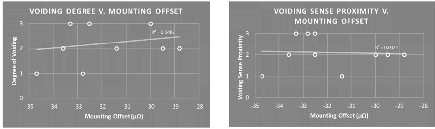
The analysis of results from ten parts is indicated below and showed no correlation with degree of voiding or with proximity to the theoretically sensitive location. It may be concluded that voiding below 20% is not found to be problematic in practice.
LIFE TIME & CONCLUSIONS
EXPECTED OHMIC VALUES DURING LIFE
The final consideration for a design engineer relying on a sub-milliohm resistor for accurate current measurements is how the ohmic value may change during the life of the product. These changes fall into two categories: reversible and irreversible.
Firstly, reversible changes occur because of the finite TCR. This is a combination of the resistance element TCR and the termination TCR and it is important not to rely too much on the element TCR stated on some datasheets, by wrongly assuming it relates to the whole product. As TCR of these parts is normally tested by manufacturers in the mounted state, it also includes the TCR for the solder between mounting pad and termination. In applications with minimal self-heating, the TCR simply reflects worst case value changes across the local ambient temperature range of the resistor. Where self-heating is greater, it becomes an issue of non-linearity since ohmic value becomes a function of current. This is sometimes expressed in terms of Power Coefficient of Resistance (PCR) which combines the temperature rise per watt with the TCR to indicate the sensitivity of ohmic value to power, measured in ppm/W. This is clearly a function of the mounting conditions as the temperature rise depends on the wider thermal environment.
Secondly, irreversible changes occur due to changes in the element resistance. Corrosion and oxidation can consume some of the resistance alloy, leading to upward value drift, whilst grain boundary changes within the alloy can cause resistivity changes which are accelerated by elevated temperatures.
A number of figures are given in the performance data of product datasheets to enable the designer to assess the maximum lifetime change in resistance value. In general, only one of these figures should be used; the one that most closely reflects operating conditions. A Shelf Life figure applies where loading is negligible, and the environment is benign. The Load or Endurance figure applies where power dissipation is the main factor, the Long-Term Damp Heat figure where humid environments may be encountered. In all these tests the majority of the value change happens within the period of the test, as the value will tend to stabilise. For example, the 1000-hour Load figure is a good guide to the change predicted over a longer period of service.
The figure of most interest to designers is the maximum total error in resistance value at the end of product life, or before scheduled re-calibration, if applicable. This is termed the total excursion and is the root of the sum of the squares of applicable, statistically independent short-term and long-term factors. This is best illustrated by an example.
An LRMAP2512 resistor with 1% tolerance and TCR of 50ppm/°C is to be soldered to a PCB for use in a laboratory-based power supply. The mean current through the resistor during operation will dissipate over 50% of the rated power. The operating temperature range inside the equipment is 20 to 50°C.
Short-Term Factors
Tolerance ±1%
TCR ±0.15% (±50ppm/°C x 30°C)
Soldering ±0.3% typical
Long-Term
Load at Rated Power ±0.3% typical
√ (12 + 0.152 + 0.32 + 0.32) = 1.1
Total Excursion Estimate: ±1.1% typical
Clearly if initial calibration can be used, this can eliminate tolerance and soldering process induced errors, and this gives:
√ (0.152 + 0.32) = 0.34
Calibrated Total Excursion: ±0.34% typical
SUMMARY AND CONCLUSIONS
The growing use of sub-milliohm chip resistors for current sensing brings challenges for the designer and the process engineer at multiple stages which need to be well understood. The component format should first of all be selected to support the chosen thermal management approach, with metal element flat chip resistors having two terminals being the most cost-effective solution. Next, it is essential to design the PCB tracks and pads to meet the needs of Kelvin connection, heat dissipation, and avoidance of induced noise. Thirdly, if it is necessary to make accurate measurement of unmounted components’ ohmic value, great care is needed to set up fixturing according to the manufacturer’s guidelines and to establish a capable test system. Next the assembly processes of solder paste application and pick and place require close control to ensure consistent solder thickness and component location. And finally, how the ohmic value may change should be evaluated, in order to establish the expected range of mounted values across the product life.
REFERENCES
[1] Optimize High-Current Sensing Accuracy by Improving Pad Layout of Low-Value Shunt Resistors; Marcus O’Sullivan; Analog Dialogue 46-06 Back Burner, June (2012); www.analog.com/analogdialogue
[2] The Truth about Placement Accuracy; Patrick Folmar; SST Semiconductor Digest; https://sst.semiconductor-digest.com/2000/04/the-truth-about-placement-accuracy/