Passive Components Blog
No Result
View All Result
  • Home
  • NewsFilter
    • All
    • Aerospace & Defence
    • Antenna
    • Applications
    • Automotive
    • Capacitors
    • Circuit Protection Devices
    • electro-mechanical news
    • Filters
    • Fuses
    • Inductors
    • Industrial
    • Integrated Passives
    • inter-connect news
    • Market & Supply Chain
    • Market Insights
    • Medical
    • Modelling and Simulation
    • New Materials & Supply
    • New Technologies
    • Non-linear Passives
    • Oscillators
    • Passive Sensors News
    • Resistors
    • RF & Microwave
    • Telecommunication
    • Weekly Digest

    Smoltek CNF-MIM Capacitors Hit 1,000x Lower Leakage

    DigiKey Expands Line Card with 108K Stock Parts and 364 Suppliers

    Würth Elektronik Announces Partner Program

    Vishay Releases Compact 0806 Low‑DCR Power Inductor

    Murata Opens New Ceramic Capacitor Manufacturing and R&D Center in Japan

    Murata Publishes Power Delivery Guide for AI Servers

    Selecting Current Sense Transformers with Würth Elektronik REDEXPERT

    Mechanical Drift Indicator of Tantalum Capacitor Anodes Degradation under Reverse Bias

    Enabling Software‑Defined Vehicle Architectures: Automotive Ethernet and Zonal Smart Power

    Trending Tags

    • Ripple Current
    • RF
    • Leakage Current
    • Tantalum vs Ceramic
    • Snubber
    • Low ESR
    • Feedthrough
    • Derating
    • Dielectric Constant
    • New Products
    • Market Reports
  • VideoFilter
    • All
    • Antenna videos
    • Capacitor videos
    • Circuit Protection Video
    • Filter videos
    • Fuse videos
    • Inductor videos
    • Inter-Connect Video
    • Non-linear passives videos
    • Oscillator videos
    • Passive sensors videos
    • Resistor videos

    Enabling Software‑Defined Vehicle Architectures: Automotive Ethernet and Zonal Smart Power

    Calculating Resistance Value of a Flyback RC Snubber 

    One‑Pulse Characterization of Nonlinear Power Inductors

    Thermistor Linearization Challenges

    Coaxial Connectors and How to Connect with PCB

    PCB Manufacturing, Test Methods, Quality and Reliability

    Transformer Behavior – Current Transfer and Hidden Feedback

    Choosing the Right Capacitor: The Importance of Accurate Measurements

    RF Inductors: Selection and Design Challenges for High-Frequency Circuits

    Trending Tags

    • Capacitors explained
    • Inductors explained
    • Resistors explained
    • Filters explained
    • Application Video Guidelines
    • EMC
    • New Products
    • Ripple Current
    • Simulation
    • Tantalum vs Ceramic
  • Knowledge Blog
  • DossiersNew
  • Suppliers
    • Who is Who
  • PCNS
    • PCNS 2025
    • PCNS 2023
    • PCNS 2021
    • PCNS 2019
    • PCNS 2017
  • Events
No Result
View All Result
Passive Components Blog
No Result
View All Result

PCB Via Design Selection; Plugging-Filling-Tenting

11.8.2025
Reading Time: 4 mins read
A A

This Würth Elektronik webinar explains some basic PCB design via selection and considerations including via clearance in the solder mask, different possibilities of via treatments and fitting selection for your application.

PCB Via Design Selection – Plugging, Filling, and Tenting

RelatedPosts

Würth Elektronik Announces Partner Program

Selecting Current Sense Transformers with Würth Elektronik REDEXPERT

Enabling Software‑Defined Vehicle Architectures: Automotive Ethernet and Zonal Smart Power

This presentation explores the principles, methodologies, and design considerations associated with PCB via structures, including plugging, filling, and tenting techniques. It provides an in-depth analysis of the via design selection process, the impact of solder mask clearances, and the implications of different via treatments per IPC-4761 standards.

1. Introduction

Printed Circuit Board (PCB) technology has evolved significantly to meet the demands for high-speed, high-density electronic applications. Vias, derived from the Latin term for “path,” play an integral role in connecting different PCB layers. This paper provides insights into via design with a focus on plugging, filling, and tenting methods, vital for enhancing mechanical reliability and electrical performance.

2. Via Design Considerations

2.1. Importance of Via Structures

Vias facilitate the electrical connection between PCB layers. Improper via management can lead to solder wicking, unreliable joints, and functional failures. Thus, the correct sealing and insulation techniques are paramount.

2.2. Via Opening and Solder Mask Clearance

Clearance design around vias in the solder mask is critical. Recommendations include maintaining a clearance of at least 250 microns around the via to account for process tolerances. This ensures reliable solder mask application, reducing risks of electrical shorts and solder leakage.

3. Methods for Via Protection

3.1. Tented Vias

Tented vias involve applying a dry film solder mask over the via. Although they prevent solder flow, they are less common in advanced German facilities due to limited mechanical reliability.

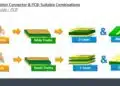
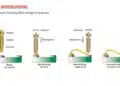
3.2. Plugged Vias (Type III and IV per IPC-4761)

  • Type III: Partial via filling using thermal curing ink via screen printing. Provides good vacuum seals but limited fine-line design applicability.
  • Type IV: Similar to Type III but covered with solder mask, providing extra isolation.

3.3. Filled Vias (Type V, VI, and VII)

  • Type V and VI: Fully filled with non-conductive epoxy, offering excellent vacuum seals and flat surfaces post-sanding.
  • Type VII: Filled and capped vias allow soldering directly on the via, supporting via-in-pad designs for high-density applications.

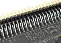
4. Manufacturing Processes

4.1. Drilling and Metallization

Vias are drilled and metallized through galvanic processes, applying copper layers within holes and on the PCB surface.

4.2. Filling Techniques

Vias are filled under vacuum to ensure void-free encapsulation. The filling materials are cured thermally, followed by surface grinding to achieve planar finishes.

4.3. Cap Plating for Type VII Vias

An additional metallization step creates a cap on filled vias, enhancing mechanical strength and thermal conductivity.

5. Design Rules and Material Considerations

5.1. Aspect Ratio

Maintaining optimal aspect ratios (drill diameter to PCB thickness) ensures process reliability.

5.2. Copper Thickness and Thermal Management

Copper wrap requirements and thermal expansion coefficients are critical in high-reliability applications. Material selection must align with these mechanical demands to prevent fatigue failures over thermal cycling.
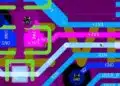
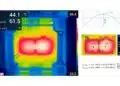
6. Applications

  • Thermal Vias: For heat dissipation in high-power components.
  • HDI Designs: Stacked microvias for compact, high-speed layouts.
  • Vacuum Testing: Ensuring airtight seals in testing environments.

7. Conclusion

Selecting the appropriate via design—whether plugged, filled, or tented—depends on the specific PCB application requirements. Early collaboration with PCB manufacturers is recommended to optimize design for manufacturability and performance.

References

  • IPC-4761: Design Guide for Protection of Printed Board Via Structures
  • IPC-6012: Qualification and Performance Specification for Rigid Printed Boards

Related

Source: Würth Elektronik

Recent Posts

Coaxial Connectors and How to Connect with PCB

17.12.2025
245

PCB Manufacturing, Test Methods, Quality and Reliability

17.12.2025
133

Connector PCB Design Challenges

3.10.2025
68

What Track Width To Use When Routing PCB

6.6.2025
124

IPC Class 2 vs Class 3 Solder Joints Requirements Explained

27.2.2025
1k

How to Determine Chip Temperature

3.1.2025
347

Die and Wire PCB Bonding Explained

1.7.2025
248

EMI Shielding Challenges

1.7.2025
23

EMC with Electromechanical Inter-Connections

1.7.2025
26

Upcoming Events

Feb 11
16:00 - 17:00 CET

What’s Next in Power Electronics Design

Feb 24
16:00 - 17:00 CET

Designing Qi2 Wireless Power Systems: Practical Development and EMC Optimization

Mar 3
16:00 - 17:00 CET

Cybersecurity at the Eleventh Hour – from RED to CRA – Information and Discussion

View Calendar

Popular Posts

  • Buck Converter Design and Calculation

    0 shares
    Share 0 Tweet 0
  • Boost Converter Design and Calculation

    0 shares
    Share 0 Tweet 0
  • LLC Resonant Converter Design and Calculation

    0 shares
    Share 0 Tweet 0
  • Flyback Converter Design and Calculation

    0 shares
    Share 0 Tweet 0
  • How Metal Prices Are Driving Passive Component Price Hikes

    0 shares
    Share 0 Tweet 0
  • Ripple Current and its Effects on the Performance of Capacitors

    3 shares
    Share 3 Tweet 0
  • Dual Active Bridge (DAB) Topology

    0 shares
    Share 0 Tweet 0
  • MLCC and Ceramic Capacitors

    0 shares
    Share 0 Tweet 0
  • What is a Dielectric Constant and DF of Plastic Materials?

    4 shares
    Share 4 Tweet 0
  • Degradation of Capacitors and its Failure Mechanisms

    0 shares
    Share 0 Tweet 0

Newsletter Subscription


Passive Components Blog

© EPCI - Leading Passive Components Educational and Information Site

  • Home
  • Privacy Policy
  • EPCI Membership & Advertisement
  • About

No Result
View All Result
  • Home
  • Knowledge Blog
  • PCNS

© EPCI - Leading Passive Components Educational and Information Site

This website uses cookies. By continuing to use this website you are giving consent to cookies being used. Visit our Privacy and Cookie Policy.
Go to mobile version